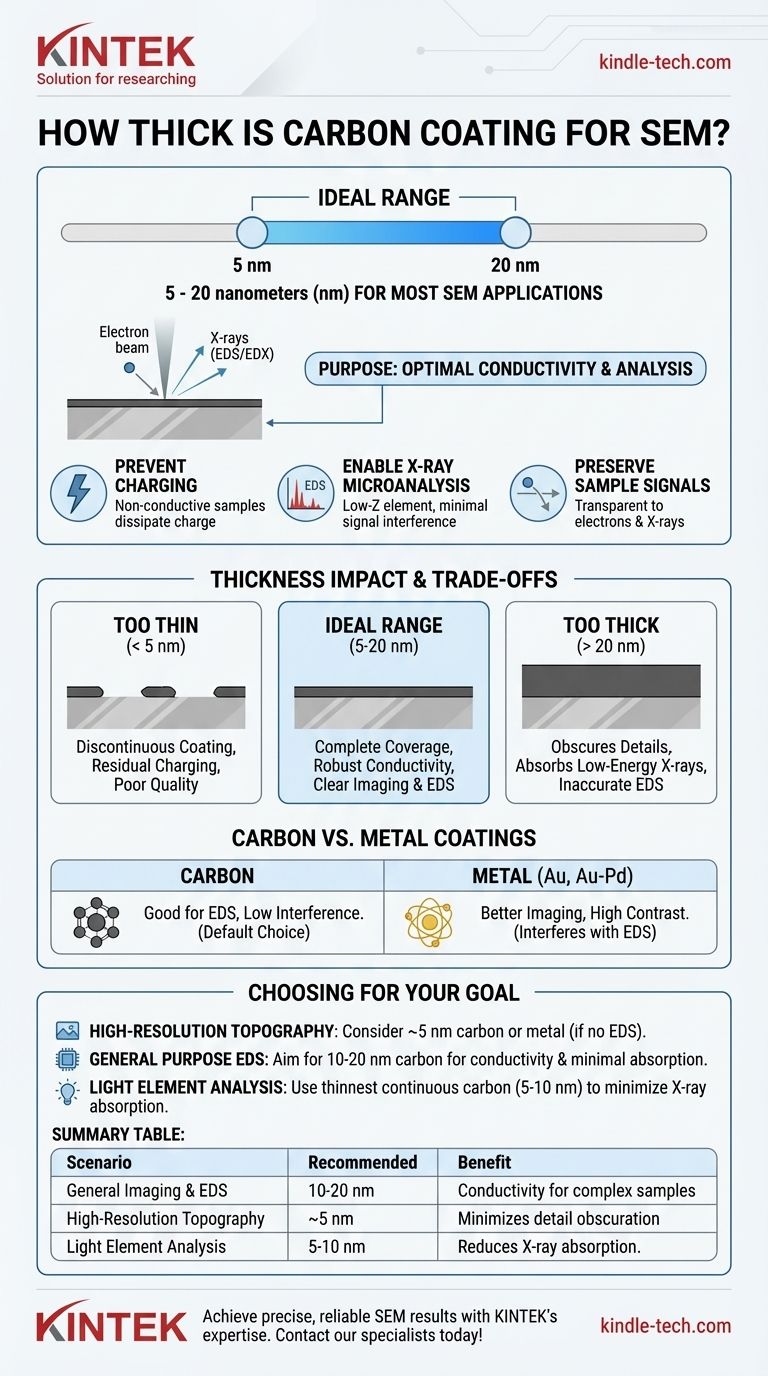
For most SEM applications, a carbon coating is typically applied at a thickness of 5 to 20 nanometers (nm). This ultrathin, conductive layer is crucial for preparing non-conductive samples for analysis, primarily by preventing electron charge buildup and enabling accurate X-ray microanalysis (EDS/EDX).
The goal of carbon coating is not to achieve a specific thickness for its own sake, but to create the thinnest possible layer that provides sufficient electrical conductivity without obscuring sample detail or interfering with analysis.
The Purpose of Carbon Coating in SEM
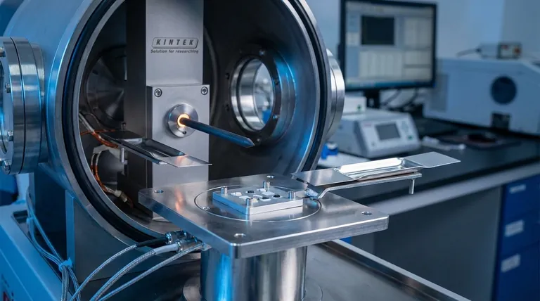
To understand why a specific thickness is used, you must first understand the fundamental problems that carbon coating solves. The process involves heating a carbon source (a rod or thread) in a vacuum, which deposits a fine, amorphous carbon film onto the specimen.
Preventing "Charging" Artifacts
Non-conductive samples, such as ceramics, polymers, or biological tissues, cannot dissipate the electrical charge from the electron beam. This accumulation of electrons, known as charging, causes bright patches, image distortion, and drift, making useful analysis impossible. A thin carbon layer provides a conductive path for this charge to flow away to the grounded sample holder.
Enabling X-ray Microanalysis (EDS/EDX)
Carbon is a low-atomic-number (low-Z) element. When the electron beam strikes the sample, it generates X-rays characteristic of the elements present. A key advantage of carbon is that its own X-ray signal is very low in energy and does not overlap with the signals of most other elements, ensuring the elemental analysis of your sample remains clear and accurate.
Preserving Sample Signals
The coating must be thin enough to be effectively transparent to electrons and X-rays. The incoming electron beam must pass through the carbon to interact with the specimen, and the resulting secondary electrons (for imaging) and X-rays (for analysis) must escape to be detected.
How Coating Thickness Impacts Analysis
The precise thickness of the carbon film is a balance between achieving conductivity and preserving the original signal from the sample.
Too Thin (< 5 nm)
An extremely thin coating risks being discontinuous. Instead of a uniform layer, it may form isolated "islands" of carbon. This provides an incomplete conductive path, leading to residual charging and poor-quality images or analysis.
The Ideal Range (5-20 nm)
This range is the standard for most applications. A 5-10 nm film is often sufficient for basic imaging and EDS on relatively flat samples. A slightly thicker coat of 10-20 nm ensures complete coverage and robust conductivity, which is ideal for samples with complex topography or when performing quantitative X-ray analysis.
Too Thick (> 20 nm)
An excessively thick coating introduces significant problems. It can obscure fine surface details, reducing the resolution of your image. More critically, it can absorb low-energy X-rays emitted by lighter elements in your sample (like sodium, magnesium, or aluminum), leading to inaccurate or completely missed elemental detection.
Understanding the Trade-offs
Choosing a coating is about making an informed compromise based on your analytical goals. No single solution is perfect for every scenario.
Carbon vs. Metal Coatings
Other materials, like gold (Au) or gold-palladium (Au-Pd), are also used for SEM coating. Metals are more conductive than carbon and yield more secondary electrons, producing sharper, higher-contrast images of surface topography.
However, the X-ray peaks from these heavy metals interfere with the EDS signals of many other elements, making them unsuitable for most microanalysis work. Carbon is the default choice when you need to know what your sample is made of.
Application Quality Matters
The thickness measurement is only a proxy for quality. The effectiveness of the coating also depends on the quality of the vacuum in the coater and the cleanliness of the process. A poor vacuum can lead to a contaminated, less conductive film, even at the "correct" thickness.
Choosing the Right Thickness for Your Goal
Select your coating strategy based on the information you need to extract from your sample.
- If your primary focus is high-resolution imaging of surface topography: Consider a very thin (5 nm) carbon coat, or use a metal coater (like gold-palladium) if EDS is not required.
- If your primary focus is general-purpose X-ray analysis (EDS/EDX): Aim for a 10-20 nm carbon coating to ensure complete conductivity without significantly absorbing most X-ray signals.
- If you are analyzing for very light elements (e.g., Na, Mg, F): Use the thinnest possible continuous carbon film (5-10 nm) to minimize the absorption of their low-energy X-rays.
A well-applied carbon coat is the invisible foundation that enables clear, accurate analysis of your specimen's true character.
Summary Table:
| Scenario | Recommended Thickness | Key Benefit |
|---|---|---|
| General Imaging & EDS | 10-20 nm | Ensures conductivity for complex samples |
| High-Resolution Topography | ~5 nm | Minimizes detail obscuration |
| Light Element Analysis (Na, Mg) | 5-10 nm | Reduces X-ray absorption |
Achieve precise, reliable SEM results with KINTEK's expertise in lab equipment and consumables. Whether you're working with non-conductive materials or require accurate EDS analysis, our carbon coating solutions ensure optimal conductivity and minimal signal interference. Contact our specialists today to discuss your specific application and enhance your laboratory's capabilities!
Visual Guide
Related Products
- Glassy Carbon Sheet RVC for Electrochemical Experiments
- Conductive Carbon Cloth Carbon Paper Carbon Felt for Electrodes and Batteries
- Electrolytic Electrochemical Cell for Coating Evaluation
People Also Ask
- What actions and conditions are strictly prohibited when working with a glassy carbon sheet? Protect Your Investment and Data Integrity
- How can the cleanliness of a pre-treated glassy carbon sheet be verified? Ensure Accurate Electrochemical Results
- What is the recommended pre-treatment procedure for polishing a glassy carbon sheet? Achieve a Mirror-Like, Contaminant-Free Surface
- What general precautions should be taken to maintain the performance and accuracy of a glassy carbon sheet? Ensure Reliable Electrochemical Data
- What are the key characteristics of RVC glassy carbon sheets? Unlock Superior Electrochemical Performance