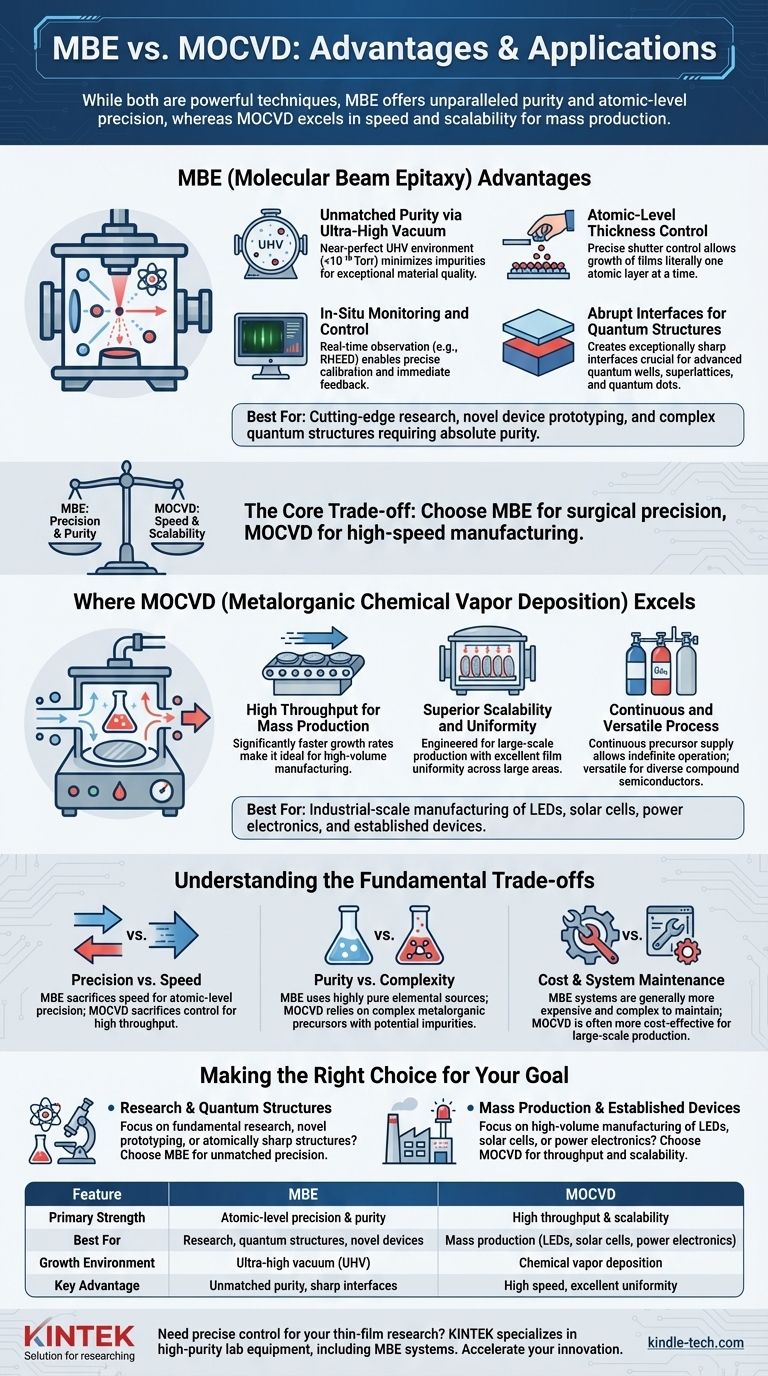
While both are powerful techniques for creating thin films, Molecular Beam Epitaxy (MBE) offers significant advantages over Metalorganic Chemical Vapor Deposition (MOCVD) in applications demanding the absolute highest material purity and atomic-level precision. This superiority stems from its ultra-high vacuum (UHV) environment and the use of elemental sources, which allows for unparalleled control over the growth process, layer by layer.
The core difference is a classic engineering trade-off. Choose MBE for its surgical precision and purity, making it ideal for cutting-edge research and complex quantum devices. Choose MOCVD for its high speed and scalability, making it the workhorse for industrial-scale manufacturing.
The Core Advantages of MBE
MBE's strengths are rooted in the physics of its environment and process. It is a method of physical vapor deposition, not chemical deposition, which creates fundamental differences in its capabilities.
Unmatched Purity via Ultra-High Vacuum
The entire MBE process occurs in an ultra-high vacuum (UHV) chamber, typically with pressures less than 10⁻¹⁰ Torr. This near-perfect vacuum means there are extremely few stray atoms or molecules to be accidentally incorporated into the growing film.
This results in semiconductor crystals of exceptional purity, which is critical for high-performance electronic and optoelectronic devices where even minor impurities can degrade performance.
Atomic-Level Thickness Control
MBE allows for the growth of films literally one atomic layer at a time. Shutters in front of the elemental sources can be opened or closed in fractions of a second, providing abrupt and precise control over material deposition.
This slow, deliberate process is what enables the creation of materials with features defined at the atomic scale, something that is much more challenging to achieve with the gas-phase chemistry of MOCVD.
In-Situ Monitoring and Control
The UHV environment of MBE is compatible with advanced real-time monitoring techniques, most notably Reflection High-Energy Electron Diffraction (RHEED).
RHEED allows operators to observe the crystalline structure of the surface as it grows. This immediate feedback enables precise calibration and control over the deposition, ensuring the desired structure is being formed atom by atom.
Abrupt Interfaces for Quantum Structures
The combination of slow growth rates and precise shutter control allows MBE to create exceptionally sharp and abrupt interfaces between different material layers.
This capability is essential for fabricating advanced heterostructures like quantum wells, superlattices, and quantum dots, where performance depends entirely on the perfection of the interfaces between layers that are only a few atoms thick.
Where MOCVD Excels
To fully appreciate MBE's advantages, it's crucial to understand the distinct strengths of MOCVD. The references highlight that MOCVD is not an inferior technique, but rather a tool optimized for a different set of goals.
High Throughput for Mass Production
MOCVD is significantly faster than MBE. Its chemical reaction-based process can deposit material at a much higher rate, making it the preferred method for high-volume manufacturing.
This is why MOCVD dominates the production of devices like LEDs and power semiconductors, where cost-per-wafer and throughput are the primary drivers.
Superior Scalability and Uniformity
MOCVD systems are engineered for large-scale production. They can handle multiple wafers at once and utilize techniques like high-speed substrate rotation (up to 1500 RPM) to ensure excellent film uniformity across large areas.
While MBE can also achieve good uniformity, MOCVD's design is inherently better suited for the demands of industrial wafer fabrication.
Continuous and Versatile Process
The process of MOCVD is continuous, as precursor gases can be supplied indefinitely without breaking vacuum. This contrasts with MBE, where the solid elemental sources eventually deplete and must be refilled, requiring a system shutdown.
MOCVD's use of a wide variety of metalorganic precursor gases also makes it highly versatile for depositing a diverse range of compound semiconductor materials.
Understanding the Fundamental Trade-offs
The choice between MBE and MOCVD is not about which is "better" overall, but which is better for a specific task. The decision hinges on three key factors.
Precision vs. Speed
This is the central conflict. MBE sacrifices speed for atomic-level precision. It is meticulous and slow, designed for creating flawless, novel structures.
MOCVD sacrifices atomic-level control for high throughput. It is fast and efficient, designed for manufacturing established device designs at scale.
Purity vs. Complexity
MBE uses highly pure elemental sources (e.g., solid gallium, arsenic), leading to ultra-pure films with a very low risk of unintentional carbon incorporation.
MOCVD relies on complex metalorganic precursor gases (e.g., trimethylgallium). While these can be highly purified, they introduce a potential source of carbon impurities and make the underlying growth chemistry more complex.
Cost and System Maintenance
MBE systems, with their required UHV technology and complex components, are generally more expensive to build and maintain per unit of throughput.
MOCVD reactors, while still highly sophisticated, are typically more cost-effective for large-scale production environments due to their higher deposition rates and simpler vacuum requirements.
Making the Right Choice for Your Goal
Your application's requirements will dictate the correct technology choice.
- If your primary focus is fundamental research, novel device prototyping, or creating atomically sharp quantum structures: MBE is the superior choice for its unmatched precision and material purity.
- If your primary focus is high-volume manufacturing of established devices like LEDs, solar cells, or power electronics: MOCVD is the industry standard due to its high throughput, scalability, and cost-effectiveness.
Ultimately, selecting the right deposition technology requires a clear understanding of whether your objective is to explore the limits of material science or to efficiently produce reliable devices at scale.
Summary Table:
| Feature | MBE (Molecular Beam Epitaxy) | MOCVD (Metalorganic Chemical Vapor Deposition) |
|---|---|---|
| Primary Strength | Atomic-level precision & purity | High throughput & scalability |
| Best For | Research, quantum structures, novel devices | Mass production (LEDs, solar cells, power electronics) |
| Growth Environment | Ultra-high vacuum (UHV) | Chemical vapor deposition |
| Key Advantage | Unmatched purity, sharp interfaces | High speed, excellent uniformity |
Need precise control for your thin-film research? KINTEK specializes in high-purity lab equipment, including MBE systems designed for cutting-edge material science. Our solutions deliver the atomic-level precision and ultra-high vacuum environments essential for developing next-generation quantum devices and semiconductor research. Contact our experts today to discuss how our equipment can accelerate your innovation.
Visual Guide
Related Products
- Electron Beam Evaporation Coating Tungsten Crucible and Molybdenum Crucible for High Temperature Applications
- Chemical Vapor Deposition CVD Equipment System Chamber Slide PECVD Tube Furnace with Liquid Gasifier PECVD Machine
- RF PECVD System Radio Frequency Plasma-Enhanced Chemical Vapor Deposition RF PECVD
People Also Ask
- What is e-beam evaporation used for? Precision Coating for Optics, Aerospace & Electronics
- What is the voltage of e-beam evaporation? Achieve Precise Thin-Film Deposition
- What is the temperature of e-beam evaporation? Mastering the Two-Zone Thermal Process for Precision Films
- What is the container that holds the metal source material called in e-beam evaporation? Ensure Purity and Quality in Your Thin-Film Deposition
- What is the deposition rate of e-beam evaporation? Control Thin Film Quality and Speed


