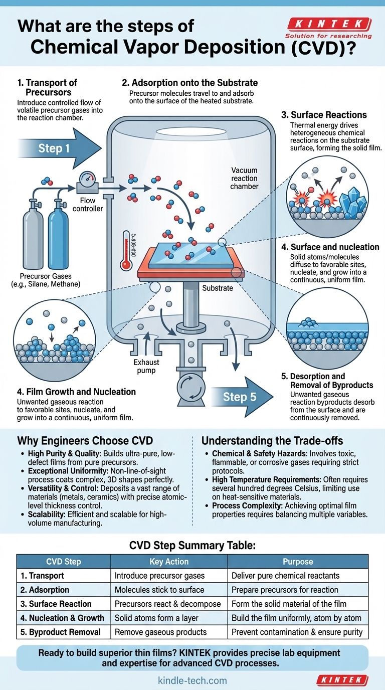
At its core, Chemical Vapor Deposition (CVD) is a process that builds a solid material, one layer of atoms at a time, from a chemical gas. The fundamental steps involve introducing reactive precursor gases into a chamber, where they decompose and react on a heated surface (the substrate) to form a high-quality thin film. Gaseous byproducts from this reaction are then removed.
Chemical Vapor Deposition is not simply a coating method; it is a bottom-up fabrication technique. By controlling chemical reactions at a molecular level, you can construct ultra-pure, exceptionally uniform thin films with properties that are impossible to achieve through traditional bulk material processing.
The Goal of CVD: Building from the Bottom Up
Chemical Vapor Deposition is a foundational process in advanced manufacturing, particularly in the semiconductor and materials science industries. Its purpose is to create highly pure and structurally perfect thin films.
Think of it as a form of molecular spray-painting. Instead of paint droplets, you use a vapor of specific chemical precursors. These precursors only react and "solidify" on the target surface, building the desired material atom by atom.
This precision is why CVD is the leading approach for manufacturing materials like graphene for high-performance electronics, where even a single atomic defect can compromise function.
A Detailed Look at the CVD Process
While the high-level concept is simple, the process itself is a sequence of carefully controlled physical and chemical events. Each step is critical to the quality of the final film.
Step 1: Transport of Precursors
The process begins by introducing one or more volatile precursor gases into a reaction chamber. The chamber is typically at a high vacuum to remove contaminants.
The flow rate, concentration, and pressure of these gases are precisely regulated, as they directly influence the speed and quality of the film's growth.
Step 2: Adsorption onto the Substrate
Once inside the chamber, the precursor gas molecules travel and land on the surface of the substrate. This initial, temporary sticking is called adsorption.
The substrate is heated to a specific temperature, which provides the energy needed for the subsequent chemical reactions to occur.
Step 3: Surface Reactions
This is the "chemical" heart of the process. The thermal energy from the heated substrate causes the adsorbed precursor molecules to decompose and/or react with each other.
These heterogeneous surface reactions are catalyzed by the surface itself, breaking chemical bonds and forming new, non-volatile (solid) species that will become the film.
Step 4: Film Growth and Nucleation
The newly formed solid atoms or molecules are not yet a uniform film. They diffuse across the surface to energetically favorable locations, known as nucleation sites.
From these sites, the film begins to grow, eventually forming a continuous, uniform, and often crystalline layer across the entire substrate. The process is controlled to create films as thin as a single layer of atoms.
Step 5: Desorption and Removal of Byproducts
The chemical reactions that form the solid film also create unwanted gaseous byproducts. These byproduct molecules must detach from the surface in a process called desorption.
A continuous flow of gas or a vacuum system then transports these byproducts out of the reaction chamber, preventing them from contaminating the growing film.
Why Engineers Choose CVD
CVD is chosen over other deposition methods when the quality, purity, and structure of the film are paramount. Its advantages are rooted in its chemical nature.
High Purity and Quality
Because it builds the material from pure chemical precursors in a controlled environment, CVD can produce films with extremely high purity and a low count of structural defects.
Exceptional Uniformity and Coverage
CVD is a non-line-of-sight process. The gas precursors flow and conform to any shape, allowing for a completely uniform coating on complex, three-dimensional surfaces—something line-of-sight methods like sputtering cannot achieve.
Versatility and Control
The process is incredibly versatile. By changing the precursor gases, temperature, and pressure, engineers can deposit a vast range of materials, including metals, ceramics, and polymers. It offers precise control over film thickness, down to the atomic scale.
Scalability and Efficiency
Compared to some other high-vacuum techniques, CVD is relatively affordable, has a high deposition rate, and is simple to scale up for high-volume manufacturing, making it economically viable.
Understanding the Trade-offs
While powerful, CVD is not without its challenges. Understanding its limitations is crucial for successful implementation.
Chemical and Safety Hazards
CVD often relies on precursor gases that are toxic, flammable, or corrosive. This necessitates sophisticated safety protocols, gas handling systems, and exhaust management, adding to the complexity and cost of the setup.
High Temperature Requirements
Many CVD processes require high substrate temperatures (often several hundred degrees Celsius) to drive the necessary chemical reactions. This can damage or deform temperature-sensitive substrate materials, limiting its application for certain plastics or pre-processed electronics.
Process Optimization Complexity
Achieving the desired film properties requires a delicate balance of multiple variables: gas flow, chamber pressure, temperature uniformity, and precursor chemistry. Developing a stable and repeatable process for a new material can be a complex and time-consuming task.
Making the Right Choice for Your Goal
Selecting a deposition technique depends entirely on your end goal.
- If your primary focus is producing high-performance electronics or sensors: CVD is ideal for creating the ultra-pure, low-defect, and atomically thin films required.
- If your primary focus is coating complex, three-dimensional parts: CVD's non-line-of-sight nature provides uniform coverage that is unmatched by other methods.
- If your primary focus is creating highly durable and pure surface coatings: CVD is a scalable and efficient method for depositing dense, high-purity films with excellent adhesion.
Ultimately, Chemical Vapor Deposition empowers engineers to build superior materials from the molecule up, enabling the next generation of advanced technologies.
Summary Table:
| CVD Step | Key Action | Purpose |
|---|---|---|
| 1. Transport | Introduce precursor gases into chamber | Deliver pure chemical reactants to the substrate |
| 2. Adsorption | Gas molecules stick to heated substrate | Prepare precursors for surface reaction |
| 3. Surface Reaction | Precursors decompose & react on substrate | Form the solid material of the thin film |
| 4. Nucleation & Growth | Solid atoms form a continuous layer | Build the film uniformly, atom by atom |
| 5. Byproduct Removal | Remove gaseous reaction products | Prevent contamination and ensure film purity |
Ready to build superior thin films for your lab?
KINTEK specializes in providing the precise lab equipment and consumables needed for advanced Chemical Vapor Deposition processes. Whether you are developing next-generation semiconductors, high-performance sensors, or durable surface coatings, our expertise ensures you have the right tools for success.
We understand that achieving ultra-pure, uniform films requires reliable and controlled processes. Let KINTEK be your partner in precision.
Contact our experts today to discuss how we can support your specific laboratory needs and help you achieve breakthrough results.
Visual Guide
Related Products
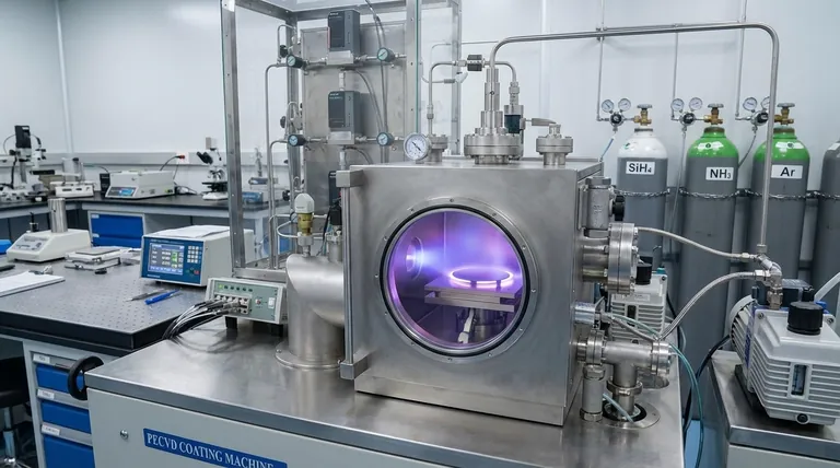
- Chemical Vapor Deposition CVD Equipment System Chamber Slide PECVD Tube Furnace with Liquid Gasifier PECVD Machine
- Microwave Plasma Chemical Vapor Deposition MPCVD Machine System Reactor for Lab and Diamond Growth
- 915MHz MPCVD Diamond Machine Microwave Plasma Chemical Vapor Deposition System Reactor
- Customer Made Versatile CVD Tube Furnace Chemical Vapor Deposition Chamber System Equipment
- HFCVD Machine System Equipment for Drawing Die Nano-Diamond Coating
People Also Ask
- What happens during deposition chemistry? Building Thin Films from Gaseous Precursors
- What is plasma enhanced chemical vapor deposition PECVD equipment? A Guide to Low-Temperature Thin Film Deposition
- How are carbon nanotubes grown? Master Scalable Production with Chemical Vapor Deposition
- How expensive is chemical vapor deposition? Understanding the True Cost of High-Performance Coating
- What is the chemical vapor deposition growth process? Build Superior Thin Films from the Atom Up


