At its core, Chemical Vapor Deposition (CVD) is a family of processes, not a single method. The primary techniques are differentiated by how they supply the energy needed to trigger the chemical reaction that forms the thin film. The three most common techniques are Thermal CVD, which uses high heat; Plasma-Enhanced CVD (PECVD), which uses an ionized gas; and Laser CVD (LCVD), which uses focused light.
The choice of a CVD technique is fundamentally a decision about the energy source. This choice dictates a critical trade-off between the processing temperature your material can withstand, the quality of the resulting film, and the specific requirements of your application.
The Guiding Principle: Energy In, Film Out
Chemical Vapor Deposition works by introducing one or more volatile precursor gases into a reaction chamber containing the object to be coated, known as the substrate.
The Universal CVD Process
Energy is then applied to the system. This energy breaks down the precursor gases, which then react and deposit onto the substrate surface as a new, solid thin film. The key difference between CVD methods lies in the type of energy used.
The Role of the Precursor
The precursor is the chemical starting point. It must be a substance that can be turned into a vapor and transported into the reactor. The final film can be made of a vast array of materials, including metals like tungsten, semiconductors like silicon, or hard coatings like titanium nitride.
A Breakdown of Major CVD Techniques
The energy source not only defines the technique but also its primary advantages and limitations.
Thermal CVD: The High-Temperature Workhorse
This is the most traditional form of CVD. It relies purely on high temperatures, often exceeding 1000°C (1925°F), to provide the activation energy for the chemical reaction.
Because it is conceptually simple and can produce high-quality films at a fast deposition rate (especially at atmospheric pressure, known as APCVD), it is widely used for applications where the substrate can tolerate extreme heat.
Plasma-Enhanced CVD (PECVD): The Low-Temperature Solution
PECVD addresses the primary limitation of thermal CVD: high temperature. Instead of just heat, it uses an electric field to create a plasma (an ionized gas) inside the chamber.
This highly energetic plasma provides the energy to break down precursor gases, allowing deposition to occur at significantly lower temperatures. This makes PECVD essential for coating temperature-sensitive materials like plastics, polymers, and many electronic components. It is also known for producing films that conform well to complex surface topographies ("good step coverage").
Laser CVD (LCVD): The Precision Tool
LCVD uses a focused laser beam to heat a highly localized area on the substrate. The chemical reaction and subsequent deposition only occur where the laser is pointed.
This technique is not for coating large areas. Instead, it is a direct-write process used for precision tasks like repairing microcircuits, prototyping, or creating specific, small-scale patterns without the need for masks.
Understanding the Trade-offs
No single CVD technique is universally superior. The choice involves balancing key performance characteristics against process limitations.
Key Advantages of CVD
- Material Versatility: CVD can deposit a wide range of materials, including metals, semiconductors, ceramics (carbides, nitrides), and carbons (like diamond and graphene).
- Strong Adhesion: The process creates a direct chemical and metallurgical bond between the film and the substrate, resulting in a very durable coating.
- High Purity & Quality: With precise control over gas purity and process conditions, CVD can produce highly pure, dense films with various microstructures (amorphous, polycrystalline, or monocrystalline).
- Reproducibility: Modern CVD systems offer excellent process control, leading to highly consistent and reproducible results from run to run.
Critical Limitations and Challenges
- High Temperature Requirements: Thermal CVD can damage or destroy substrates that are not thermally stable, limiting its range of applications.
- Hazardous Chemicals: Many precursor gases used in CVD are toxic, flammable, or corrosive. This necessitates strict safety protocols for handling and disposal to protect personnel and the environment.
- Precursor Availability: While many materials can be deposited, a suitable volatile precursor must exist for that material. For some complex alloys or compounds, finding a stable and effective precursor can be a significant challenge.
- Process Byproducts: The chemical reactions can produce corrosive byproducts that may damage equipment over time, requiring careful maintenance.
Making the Right Choice for Your Application
Your primary goal will determine the most suitable CVD technique.
- If your primary focus is high-volume, general-purpose coating on a heat-tolerant substrate: Thermal CVD is often the most established and cost-effective method due to its high deposition rates.
- If your primary focus is coating temperature-sensitive electronics, polymers, or medical devices: PECVD is the definitive choice, as its low-temperature process prevents damage to the underlying substrate.
- If your primary focus is precision patterning, maskless fabrication, or circuit repair: LCVD provides unparalleled spatial control for depositing material in exact locations.
Ultimately, understanding the energy source is the key to mastering Chemical Vapor Deposition and selecting the right tool for the job.
Summary Table:
| Technique | Energy Source | Key Advantage | Ideal For |
|---|---|---|---|
| Thermal CVD | High Heat | High deposition rate, high-quality films | Heat-tolerant substrates, general-purpose coating |
| Plasma-Enhanced CVD (PECVD) | Ionized Gas (Plasma) | Low-temperature process | Temperature-sensitive materials (electronics, polymers) |
| Laser CVD (LCVD) | Focused Laser Beam | High precision, maskless patterning | Circuit repair, prototyping, precision tasks |
Ready to integrate the right CVD technique into your lab workflow?
At KINTEK, we specialize in providing high-quality lab equipment and consumables for all your deposition needs. Whether you require a robust Thermal CVD system for high-volume production or a precise PECVD setup for delicate electronics, our experts can help you select the ideal solution to enhance your research and development.
Contact us today to discuss your specific application and let KINTEK empower your laboratory's capabilities.
Visual Guide

Related Products
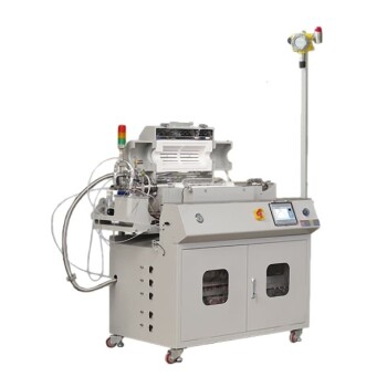
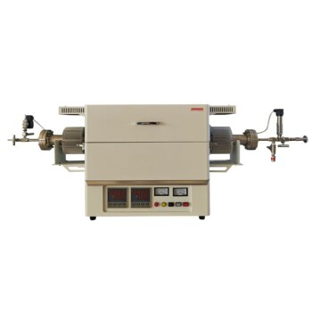
- Customer Made Versatile CVD Tube Furnace Chemical Vapor Deposition Chamber System Equipment
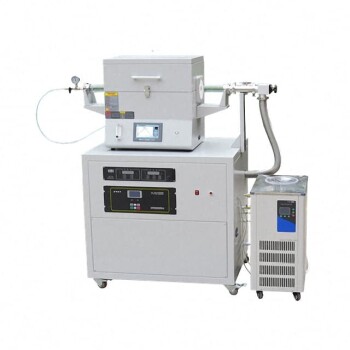
- Split Chamber CVD Tube Furnace with Vacuum Station Chemical Vapor Deposition System Equipment Machine
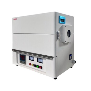
- 1200℃ Split Tube Furnace with Quartz Tube Laboratory Tubular Furnace
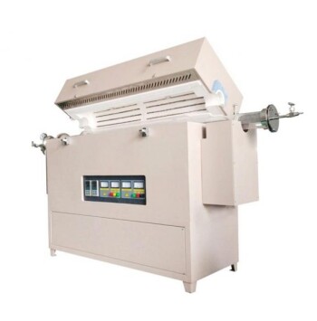
- Multi-zone Laboratory Tube Furnace
- 1400℃ Laboratory High Temperature Tube Furnace with Alumina Tube
People Also Ask
- How does chirality affect carbon nanotubes? It Determines If They Are Metal or Semiconductor
- Are all lab grown diamonds CVD? Understanding the Two Main Methods
- How high of temperature do carbon nanotubes in air have the ability to sustain? Understanding the Oxidation Limit
- What is the floating catalyst method? A Guide to High-Yield CNT Production
- Why are carbon nanotubes important in industry? Unlocking Next-Generation Material Performance
