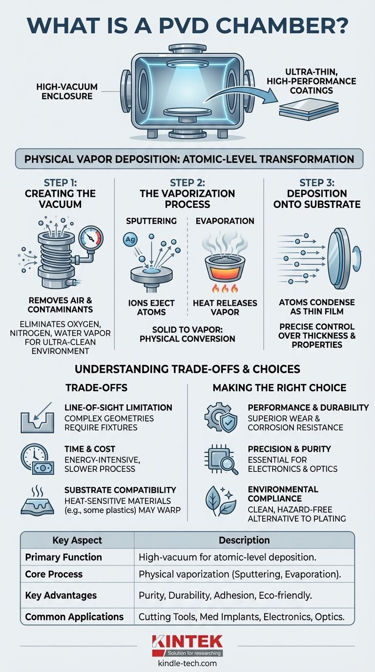
At its core, a PVD chamber is a high-vacuum enclosure designed to create ultra-thin, high-performance coatings. Inside this chamber, a solid coating material is vaporized into its atomic components, transported through the vacuum, and then condensed onto the surface of a target object, or "substrate." This highly controlled physical process—not a chemical one—is what produces coatings known for their exceptional purity, durability, and adhesion.
The PVD chamber is not merely a container; it is a precision instrument that manipulates matter at the atomic level. It uses a vacuum to create an ultra-clean environment, then employs physical energy to transform a solid material into a vapor that deposits onto a part atom by atom.
How a PVD Chamber Works: From Solid to Thin Film
The term Physical Vapor Deposition (PVD) describes a family of processes. While the specific methods vary, they all occur within the chamber and follow three fundamental steps.
Step 1: Creating the Vacuum
The first and most critical step is the removal of air and other gases from the chamber. High-power turbomolecular or cryogenic pumps create a vacuum millions of times less dense than the air we breathe.
This ultra-high vacuum is essential because it eliminates contaminants like oxygen, nitrogen, and water vapor. Any stray particles would otherwise react with the coating material and create imperfections, compromising the purity and performance of the final film.
Step 2: The Vaporization Process
Once the vacuum is established, the source material that will form the coating—often a solid block or puck of metal like titanium or chromium—must be converted into a vapor.
This is the "Physical Vapor" part of PVD. The two most common methods for achieving this are:
- Sputtering: An inert gas like argon is introduced into the chamber and ionized, creating a plasma. These high-energy ions are accelerated into the source material, acting like an atomic-scale sandblaster that ejects, or "sputters," atoms from the source.
- Evaporation: The source material is heated to its boiling point using methods like an electron-beam or a thermal resistor. As it boils, it releases a vapor of atoms that fills the chamber.
Step 3: Deposition onto the Substrate
The vaporized atoms travel in a straight line through the vacuum until they strike the cooler surface of the object being coated. Upon impact, they instantly condense back into a solid state, forming a thin, highly-adherent film.
By precisely controlling the chamber's pressure, temperature, and deposition time, engineers can manage the coating's thickness, structure, and final properties with incredible accuracy.
Understanding the Trade-offs
While powerful, the PVD process and its reliance on the chamber's design come with specific limitations that make it unsuitable for certain applications.
Line-of-Sight Limitation
Because the vaporized atoms travel in straight lines, PVD is a "line-of-sight" process. Surfaces that are hidden or inside deep, narrow cavities will not get coated effectively without complex fixtures that rotate the part during deposition.
Process Time and Cost
Creating a high-quality vacuum is an energy-intensive and time-consuming step. This, combined with the relatively slow rate of deposition for some materials, can make PVD more expensive and slower than bulk finishing methods like electroplating or painting.
Substrate Compatibility
The PVD process, particularly sputtering, can generate significant heat. This may limit its use on temperature-sensitive materials, such as certain low-melting-point plastics, which could warp or be damaged inside the chamber.
Making the Right Choice for Your Goal
Understanding the chamber's function clarifies when and why you should specify a PVD coating for your project. The decision hinges on the performance requirements of the final surface.
- If your primary focus is performance and durability: PVD is the superior choice for creating hard, wear-resistant, and corrosion-resistant surfaces on high-value components like cutting tools, medical implants, and engine parts.
- If your primary focus is precision and purity: The vacuum environment makes PVD the standard for electronics and optics, where even microscopic contamination could cause a component to fail.
- If your primary focus is environmental compliance: PVD is a clean, dry process that provides a powerful alternative to traditional electrochemical methods like hard chrome plating, which involve hazardous chemicals.
Ultimately, the PVD chamber is a tool for engineering surfaces with properties that are impossible to achieve through other means.
Summary Table:
| Key Aspect | Description |
|---|---|
| Primary Function | Creates a high-vacuum environment for atomic-level thin-film deposition. |
| Core Process | Physical vaporization of a solid material (e.g., sputtering, evaporation) onto a substrate. |
| Key Advantages | Exceptional coating purity, durability, adhesion, and environmental compliance. |
| Common Applications | Cutting tools, medical implants, electronics, optics, and engine components. |
| Main Limitations | Line-of-sight coating, higher process time/cost, heat sensitivity of some substrates. |
Ready to engineer superior surfaces with precision PVD coatings? KINTEK specializes in high-performance lab equipment and consumables, including PVD solutions tailored to your laboratory's specific needs. Our expertise ensures you achieve the purity, durability, and performance your applications demand. Contact our experts today to discuss how our PVD technology can enhance your research and development.
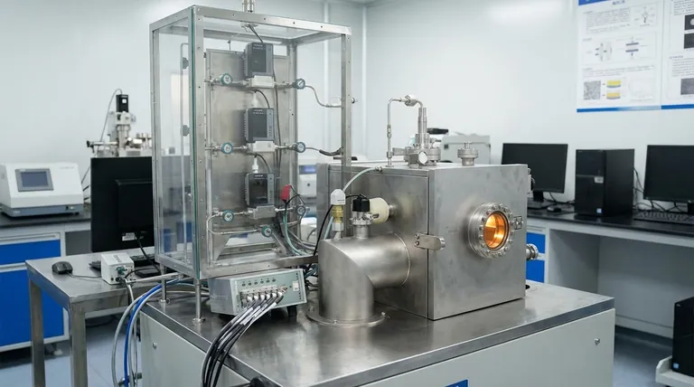
Visual Guide
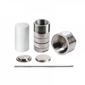
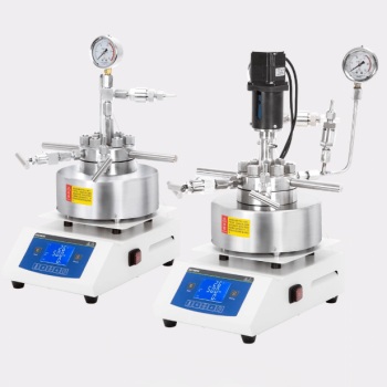
Related Products
- Inclined Rotary Plasma Enhanced Chemical Vapor Deposition PECVD Equipment Tube Furnace Machine
- RF PECVD System Radio Frequency Plasma-Enhanced Chemical Vapor Deposition RF PECVD
- Split Chamber CVD Tube Furnace with Vacuum Station Chemical Vapor Deposition System Equipment Machine
- Chemical Vapor Deposition CVD Equipment System Chamber Slide PECVD Tube Furnace with Liquid Gasifier PECVD Machine
- Customer Made Versatile CVD Tube Furnace Chemical Vapor Deposition Chamber System Equipment
People Also Ask
- What is PECVD used for? Achieve Low-Temperature, High-Performance Thin Films
- What is PECVD silicon deposition? Achieve Low-Temperature, High-Quality Thin Films
- What is meant by vapor deposition? A Guide to Atomic-Level Coating Technology
- What materials are deposited in PECVD? Discover the Versatile Thin-Film Materials for Your Application
- What is plasma enhanced chemical vapour deposition process? Unlock Low-Temperature, High-Quality Thin Films