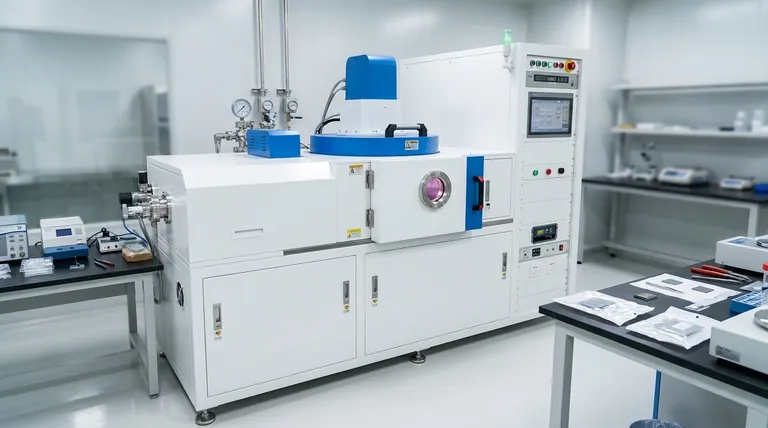
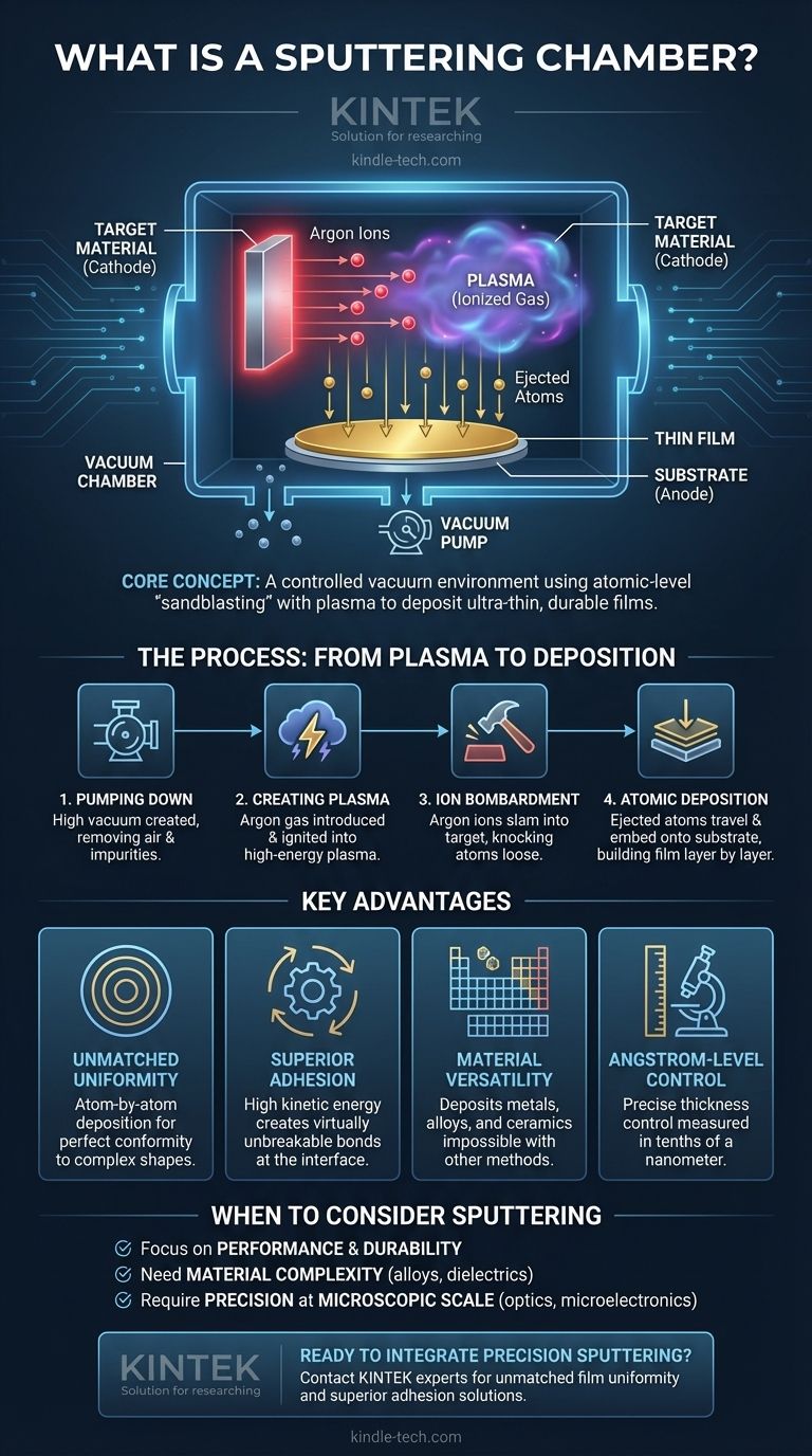
In essence, a sputtering chamber is a highly controlled vacuum environment designed for a physical vapor deposition (PVD) process called sputtering. Inside this chamber, a target material is bombarded with energized ions from a gas plasma, which physically knocks atoms loose from the target. These ejected atoms then travel through the vacuum and deposit onto a substrate, forming an exceptionally thin, uniform, and durable film.
The core challenge in advanced manufacturing is creating flawless, ultra-thin coatings with powerful adhesion. A sputtering chamber solves this by using a form of atomic-level "sandblasting" in a pure vacuum, enabling a level of precision and bond strength that other coating methods cannot achieve.
The Anatomy of the Process
To understand the chamber, you must first understand the key elements at play within it. The entire system is engineered to manage an atomic-scale process with high precision.
The Vacuum Environment
The process must occur in a high vacuum. This is critical for two reasons: it prevents atoms from the coating material from colliding with air molecules, and it removes impurities that could otherwise contaminate the film.
The Target Material
This is a block or plate of the material you wish to create a film from, such as titanium, gold, or silicon dioxide. It acts as the source for the coating atoms.
The Substrate
This is the object you intend to coat. It can be anything from a silicon wafer and an eyeglass lens to a medical implant or a drill bit.
The Ionized Gas (Plasma)
A small, controlled amount of an inert gas, almost always Argon, is introduced into the chamber. A strong electric field is then applied, stripping electrons from the Argon atoms and creating a glowing, high-energy state of matter known as plasma.
How Sputtering Deposition Works
The process is a precise sequence of events, each enabled by the design of the chamber.
Step 1: Pumping Down
First, powerful pumps remove nearly all the air from the chamber, creating a vacuum. This "pump-down" phase is essential for film purity.
Step 2: Creating the Plasma
Once a sufficient vacuum is reached, Argon gas is bled into the chamber. A high voltage is applied between the target (which acts as the cathode) and the chamber walls (anode), igniting the gas into a plasma.
Step 3: Ion Bombardment
The positively charged Argon ions in the plasma are accelerated by the electric field and slam into the negatively charged target material with tremendous force.
Step 4: Atomic Ejection and Deposition
Each impact has enough energy to physically knock atoms or molecules off the target material. These ejected particles travel in a straight line through the vacuum until they strike the substrate, embedding themselves and building up, layer by layer, into a thin film.
Understanding the Key Advantages
Sputtering is chosen over other methods when the quality and performance of the film are paramount.
Unmatched Film Uniformity
Because the material is deposited atom by atom, the resulting film has exceptional uniformity and can perfectly conform to the complex topography of a substrate.
Superior Adhesion
The sputtered atoms arrive at the substrate with high kinetic energy. This energy helps them form a dense film and creates a "virtually unbreakable bond" at the interface, as the arriving atoms physically embed into the top layer of the substrate.
Material Versatility
The physical nature of the process means that almost any material can be sputtered. This includes pure metals, alloys, and even insulating ceramic compounds, which are difficult or impossible to deposit using other methods like thermal evaporation.
Angstrom-Level Control
The thickness of the deposited film is a direct function of time and power. This allows for incredibly precise control, enabling the creation of films with thicknesses measured in angstroms (tenths of a nanometer).
When to Consider Sputtering
Choosing a deposition method depends entirely on the technical requirements of your final product.
- If your primary focus is performance and durability: Sputtering is the superior choice for creating dense, highly adherent thin films that can withstand wear and environmental stress.
- If your primary focus is material complexity: This process offers the versatility to deposit alloys, dielectrics, and refractory metals that cannot be handled by simple evaporation.
- If your primary focus is precision at a microscopic scale: Sputtering provides the atomic-level thickness control required for manufacturing optical filters, semiconductors, and other microelectronic devices.
Ultimately, understanding the sputtering chamber is to understand a foundational tool that enables much of modern materials science and high-technology manufacturing.
Summary Table:
| Key Component | Role in the Sputtering Process |
|---|---|
| Vacuum Environment | Prevents contamination and allows atoms to travel unimpeded. |
| Target Material | The source (e.g., gold, titanium) of the coating atoms. |
| Substrate | The object (e.g., silicon wafer, lens) being coated. |
| Ionized Gas (Plasma) | Provides the energetic ions (usually Argon) to eject target atoms. |
| Key Advantage | Why It Matters for Your Application |
|---|---|
| Superior Adhesion | Creates a virtually unbreakable bond for durable, high-performance coatings. |
| Unmatched Uniformity | Ensures consistent, conformal coatings even on complex geometries. |
| Material Versatility | Deposits a wide range of materials, including alloys and insulating ceramics. |
| Angstrom-Level Control | Enables precise thickness control for advanced microelectronics and optics. |
Ready to Integrate Precision Sputtering into Your Lab?
Understanding the sputtering chamber is the first step. The next is finding the right equipment to achieve your specific coating goals. KINTEK specializes in high-performance lab equipment and consumables, serving the precise needs of research and development laboratories.
Whether you are developing next-generation semiconductors, durable medical implants, or advanced optical filters, our expertise can help you select the ideal sputtering solution for unmatched film uniformity, superior adhesion, and material versatility.
Let's discuss your project requirements. Contact our experts today to find the perfect sputtering system for your laboratory's challenges.
Visual Guide
Related Products
- Split Chamber CVD Tube Furnace with Vacuum Station Chemical Vapor Deposition System Equipment Machine
- Customer Made Versatile CVD Tube Furnace Chemical Vapor Deposition Chamber System Equipment
- Chemical Vapor Deposition CVD Equipment System Chamber Slide PECVD Tube Furnace with Liquid Gasifier PECVD Machine
- Multi Heating Zones CVD Tube Furnace Machine Chemical Vapor Deposition Chamber System Equipment
People Also Ask
- What functions does a tube CVD furnace perform during the stabilization and carbonization of composite fibers?
- What is a major limitation of standard CVD? Solve the Thermal Barrier with Advanced Coating Solutions
- How does a tube CVD reactor facilitate N-CNT growth? Master Precision Synthesis on Carbon Paper
- What is a CVD tube furnace? A Complete Guide to Thin-Film Deposition
- How does a CVD tube furnace inhibit the sintering of silver supports? Boost Membrane Durability and Performance


