Knowledge cvd machine What is chemical vapor deposition growth process? A Guide to Building High-Performance Thin Films
Author avatar

Tech Team · Kintek Solution

Updated 3 months ago

What is chemical vapor deposition growth process? A Guide to Building High-Performance Thin Films


At its core, the chemical vapor deposition (CVD) growth process is a method for depositing a thin, solid film onto a surface, known as a substrate. This is achieved by placing the substrate inside a reaction chamber, introducing specific chemical precursor gases, and applying energy—typically heat—to trigger a chemical reaction that forms the desired material directly on the substrate's surface.

Chemical vapor deposition is not merely a coating technique; it is a precise, atom-by-atom construction process. It allows for the creation of exceptionally pure, high-performance materials by building them from a gaseous state, one chemical reaction at a time.

What is chemical vapor deposition growth process? A Guide to Building High-Performance Thin Films

The Fundamental Goal: Building Materials from Gas

The primary purpose of CVD is to grow solid materials with highly controlled properties. Unlike melting and casting a material, CVD builds the material from the ground up.

This bottom-up approach provides incredible control over the final product's thickness, purity, and crystalline structure. It is the go-to method for applications where material performance is paramount.

Deconstructing the CVD Process: A Step-by-Step Breakdown

While different CVD methods exist, they all follow a similar sequence of events at the microscopic level. Understanding these steps is key to controlling the final outcome.

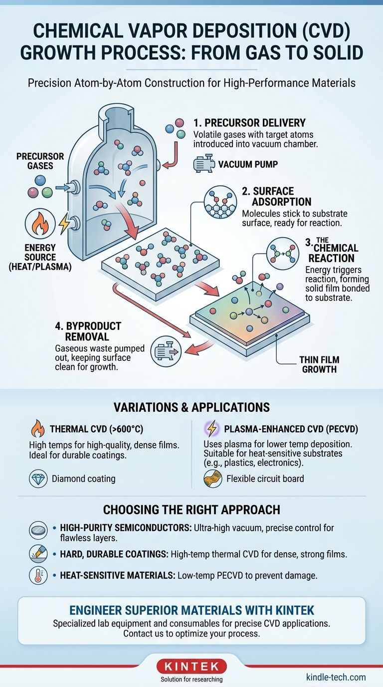
Step 1: Precursor Delivery

Volatile precursor gases, which contain the atoms needed for the final film, are injected into the reaction chamber. The chamber is typically under a vacuum to remove impurities and control the flow of these gases toward the substrate.

Step 2: Surface Adsorption

Once the precursor gas molecules reach the substrate, they stick to the surface in a process called adsorption. This is a necessary prelude to the chemical reaction.

Step 3: The Chemical Reaction

With the precursor molecules on the surface, energy (like heat) causes them to decompose or react with other gases. This reaction forms the desired solid material, which bonds directly to the substrate.

Over time, this process repeats, building up the thin film layer by layer. The nonvolatile products of the reaction are what form the film.

Step 4: Byproduct Removal

The chemical reaction also creates gaseous byproducts that are no longer needed. These waste products desorb (detach) from the surface and are transported away by the vacuum system, keeping the growth surface clean for new precursors to arrive.

Understanding the Trade-offs and Variations

CVD is not a single technique but a family of processes, each with its own advantages and limitations. The choice of method depends entirely on the desired material and the substrate being used.

Thermal CVD vs. Plasma-Enhanced CVD (PECVD)

Thermal CVD is the classic method, relying solely on high temperatures (often >600°C) to initiate the reaction. This produces very high-quality, dense films.

However, such high temperatures can damage sensitive substrates like plastics or certain electronic components. Plasma-Enhanced CVD (PECVD) solves this by using an electrical field to create a plasma, which provides the energy for the reaction. This allows deposition to occur at much lower temperatures.

The Challenge of Uniformity

A key goal of CVD is to create a film of perfectly even thickness across the entire substrate. While CVD is excellent at this, achieving perfect uniformity on complex, three-dimensional shapes can be a significant engineering challenge that requires careful control of gas flow and temperature gradients.

The Cost and Complexity

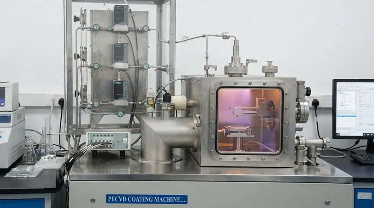
CVD systems, especially those for high-purity electronics, require sophisticated vacuum chambers, gas handling systems, and temperature controls. This makes the initial investment and operational complexity higher than simpler coating methods like painting or electroplating.

Making the Right Choice for Your Goal

Selecting the correct CVD approach requires aligning the process parameters with the application's specific needs.

  • If your primary focus is high-purity semiconductors: You must prioritize ultra-high vacuum conditions and precisely controlled precursor gases to create flawless crystalline layers.
  • If your primary focus is creating hard, durable coatings (like synthetic diamond): You should lean towards high-temperature thermal CVD variants to promote the growth of a dense, strongly bonded film.
  • If your primary focus is coating heat-sensitive materials: You must use a low-temperature method like Plasma-Enhanced CVD (PECVD) to deposit the film without damaging the underlying substrate.

By mastering these principles, you can leverage chemical vapor deposition to engineer materials with properties tailored to nearly any advanced application.

Summary Table:

Key CVD Process Step What Happens Key Outcome
Precursor Delivery Gases containing target atoms are introduced into a vacuum chamber. Precursors are delivered to the substrate surface.
Surface Adsorption Gas molecules stick (adsorb) onto the substrate surface. Precursors are in position for the reaction.
Chemical Reaction Energy (heat/plasma) triggers a reaction, forming a solid material. The desired thin film bonds to the substrate.
Byproduct Removal Gaseous waste products are pumped away from the chamber. A clean surface is maintained for continued growth.

Ready to Engineer Superior Materials with CVD?

Mastering the Chemical Vapor Deposition process is key to developing next-generation semiconductors, durable protective coatings, and high-purity materials. The right lab equipment is critical for achieving the precise control, uniformity, and purity your research demands.

KINTEK specializes in providing the advanced lab equipment and consumables you need to excel. Whether you are developing electronics, creating hard coatings, or working with heat-sensitive substrates, we have the expertise and solutions to support your specific CVD applications.

Contact us today to discuss how our products can help you optimize your CVD process and achieve breakthrough results.

Get in Touch with Our Experts

Visual Guide

What is chemical vapor deposition growth process? A Guide to Building High-Performance Thin Films Visual Guide

Related Products

People Also Ask

Related Products

Chemical Vapor Deposition CVD Equipment System Chamber Slide PECVD Tube Furnace with Liquid Gasifier PECVD Machine

Chemical Vapor Deposition CVD Equipment System Chamber Slide PECVD Tube Furnace with Liquid Gasifier PECVD Machine

KT-PE12 Slide PECVD System: Wide power range, programmable temp control, fast heating/cooling with sliding system, MFC mass flow control & vacuum pump.

Customer Made Versatile CVD Tube Furnace Chemical Vapor Deposition Chamber System Equipment

Customer Made Versatile CVD Tube Furnace Chemical Vapor Deposition Chamber System Equipment

Get your exclusive CVD furnace with KT-CTF16 Customer Made Versatile Furnace. Customizable sliding, rotating, and tilting functions for precise reactions. Order now!

Microwave Plasma Chemical Vapor Deposition MPCVD Machine System Reactor for Lab and Diamond Growth

Microwave Plasma Chemical Vapor Deposition MPCVD Machine System Reactor for Lab and Diamond Growth

Get high-quality diamond films with our Bell-jar Resonator MPCVD machine designed for lab and diamond growth. Discover how Microwave Plasma Chemical Vapor Deposition works for growing diamonds using carbon gas and plasma.

915MHz MPCVD Diamond Machine Microwave Plasma Chemical Vapor Deposition System Reactor

915MHz MPCVD Diamond Machine Microwave Plasma Chemical Vapor Deposition System Reactor

915MHz MPCVD Diamond Machine and its multi-crystal effective growth, the maximum area can reach 8 inches, the maximum effective growth area of single crystal can reach 5 inches. This equipment is mainly used for the production of large-size polycrystalline diamond films, the growth of long single crystal diamonds, the low-temperature growth of high-quality graphene, and other materials that require energy provided by microwave plasma for growth.

Custom CVD Diamond Coating for Lab Applications

Custom CVD Diamond Coating for Lab Applications

CVD Diamond Coating: Superior Thermal Conductivity, Crystal Quality, and Adhesion for Cutting Tools, Friction, and Acoustic Applications

Split Chamber CVD Tube Furnace with Vacuum Station Chemical Vapor Deposition System Equipment Machine

Split Chamber CVD Tube Furnace with Vacuum Station Chemical Vapor Deposition System Equipment Machine

Efficient split chamber CVD furnace with vacuum station for intuitive sample checking and quick cooling. Up to 1200℃ max temperature with accurate MFC mass flowmeter control.

HFCVD Machine System Equipment for Drawing Die Nano-Diamond Coating

HFCVD Machine System Equipment for Drawing Die Nano-Diamond Coating

The nano-diamond composite coating drawing die uses cemented carbide (WC-Co) as the substrate, and uses the chemical vapor phase method ( CVD method for short ) to coat the conventional diamond and nano-diamond composite coating on the surface of the inner hole of the mold.

CVD Diamond for Thermal Management Applications

CVD Diamond for Thermal Management Applications

CVD diamond for thermal management: High-quality diamond with thermal conductivity up to 2000 W/mK, ideal for heat spreaders, laser diodes, and GaN on Diamond (GOD) applications.

RF PECVD System Radio Frequency Plasma-Enhanced Chemical Vapor Deposition RF PECVD

RF PECVD System Radio Frequency Plasma-Enhanced Chemical Vapor Deposition RF PECVD

RF-PECVD is an acronym for "Radio Frequency Plasma-Enhanced Chemical Vapor Deposition." It deposits DLC (Diamond-like carbon film) on germanium and silicon substrates. It is utilized in the 3-12um infrared wavelength range.

Multi Heating Zones CVD Tube Furnace Machine Chemical Vapor Deposition Chamber System Equipment

Multi Heating Zones CVD Tube Furnace Machine Chemical Vapor Deposition Chamber System Equipment

KT-CTF14 Multi Heating Zones CVD Furnace - Precise Temperature Control and Gas Flow for Advanced Applications. Max temp up to 1200℃, 4 channels MFC mass flow meter, and 7" TFT touch screen controller.

Cylindrical Resonator MPCVD Machine System Reactor for Microwave Plasma Chemical Vapor Deposition and Lab Diamond Growth

Cylindrical Resonator MPCVD Machine System Reactor for Microwave Plasma Chemical Vapor Deposition and Lab Diamond Growth

Learn about Cylindrical Resonator MPCVD Machine, the microwave plasma chemical vapor deposition method used for growing diamond gemstones and films in the jewelry and semi-conductor industries. Discover its cost-effective advantages over traditional HPHT methods.

Inclined Rotary Plasma Enhanced Chemical Vapor Deposition PECVD Equipment Tube Furnace Machine

Inclined Rotary Plasma Enhanced Chemical Vapor Deposition PECVD Equipment Tube Furnace Machine

Upgrade your coating process with PECVD coating equipment. Ideal for LED, power semiconductors, MEMS and more. Deposits high-quality solid films at low temps.

CVD Diamond Dressing Tools for Precision Applications

CVD Diamond Dressing Tools for Precision Applications

Experience the Unbeatable Performance of CVD Diamond Dresser Blanks: High Thermal Conductivity, Exceptional Wear Resistance, and Orientation Independence.

CVD Diamond Wire Drawing Die Blanks for Precision Applications

CVD Diamond Wire Drawing Die Blanks for Precision Applications

CVD diamond wire drawing die blanks: superior hardness, abrasion resistance, and applicability in wire drawing various materials. Ideal for abrasive wear machining applications like graphite processing.

CVD Diamond Cutting Tool Blanks for Precision Machining

CVD Diamond Cutting Tool Blanks for Precision Machining

CVD Diamond Cutting Tools: Superior Wear Resistance, Low Friction, High Thermal Conductivity for Non-Ferrous Materials, Ceramics, Composites Machining

Inclined Rotary Plasma Enhanced Chemical Vapor Deposition PECVD Equipment Tube Furnace Machine

Inclined Rotary Plasma Enhanced Chemical Vapor Deposition PECVD Equipment Tube Furnace Machine

Introducing our inclined rotary PECVD furnace for precise thin film deposition. Enjoy automatic matching source, PID programmable temperature control, and high accuracy MFC mass flowmeter control. Built-in safety features for peace of mind.

Laboratory CVD Boron Doped Diamond Materials

Laboratory CVD Boron Doped Diamond Materials

CVD boron-doped diamond: A versatile material enabling tailored electrical conductivity, optical transparency, and exceptional thermal properties for applications in electronics, optics, sensing, and quantum technologies.

Electron Beam Evaporation Coating Oxygen-Free Copper Crucible and Evaporation Boat

Electron Beam Evaporation Coating Oxygen-Free Copper Crucible and Evaporation Boat

Electron Beam Evaporation Coating Oxygen-Free Copper Crucible enables precise co-deposition of various materials. Its controlled temperature and water-cooled design ensure pure and efficient thin film deposition.

Hemispherical Bottom Tungsten Molybdenum Evaporation Boat

Hemispherical Bottom Tungsten Molybdenum Evaporation Boat

Used for gold plating, silver plating, platinum, palladium, suitable for a small amount of thin film materials. Reduce the waste of film materials and reduce heat dissipation.

Molybdenum Tungsten Tantalum Evaporation Boat for High Temperature Applications

Molybdenum Tungsten Tantalum Evaporation Boat for High Temperature Applications

Evaporation boat sources are used in thermal evaporation systems and are suitable for depositing various metals, alloys and materials. Evaporation boat sources are available in different thicknesses of tungsten, tantalum and molybdenum to ensure compatibility with a variety of power sources. As a container, it is used for vacuum evaporation of materials. They can be used for thin film deposition of various materials, or designed to be compatible with techniques such as electron beam fabrication.


Leave Your Message