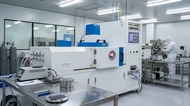
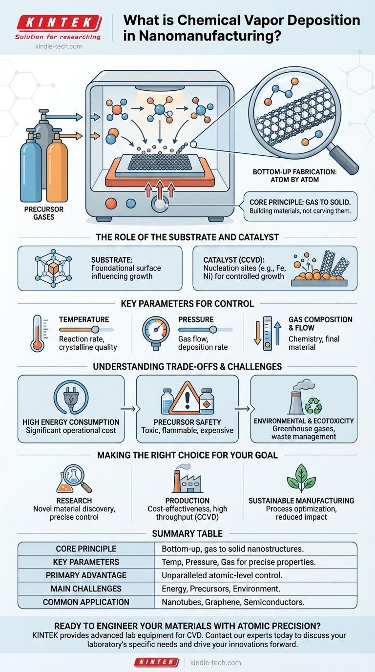
In the world of nanomanufacturing, Chemical Vapor Deposition (CVD) is a highly controlled, bottom-up fabrication process used to build nanoscale materials from the atom up. It involves introducing chemical precursor gases into a reaction chamber where they react and deposit onto a surface (a substrate), forming a high-purity thin film or a specific nanostructure, such as a carbon nanotube. This method is foundational for creating advanced materials with precisely engineered properties.
Chemical Vapor Deposition is not merely a coating technique; it is the architectural tool of nanotechnology. It grants immense control over material structure at the atomic level, but this precision requires a deliberate balance of cost, energy consumption, and environmental impact.
How Chemical Vapor Deposition Works at the Nanoscale
CVD operates on a simple but powerful principle: transforming gas into a solid. This "bottom-up" approach is fundamentally different from "top-down" methods like etching, as it involves building materials rather than carving them away.
The Core Principle: Gas to Solid
The process begins by introducing one or more volatile precursor gases into a vacuum chamber containing the substrate. When these gases are heated, they decompose and undergo chemical reactions near or on the substrate surface. The solid products of these reactions then deposit onto the substrate, gradually building the desired nanoscale material layer by layer.
The Role of the Substrate and Catalyst
The substrate is the foundational surface where the material growth occurs. Its properties, such as temperature and crystal structure, can influence the final product.
In many applications, especially for creating structures like carbon nanotubes, a catalyst is used. This is known as Catalytic CVD (CCVD). A thin layer of catalyst material (like iron or nickel nanoparticles) is placed on the substrate, serving as a nucleation site that directs and accelerates the growth of the nanostructure with a high degree of control.
Key Parameters for Control
The power of CVD lies in its tunability. By precisely adjusting key parameters, engineers can dictate the final material's characteristics:
- Temperature: Affects the reaction rate and the crystalline quality of the deposited material.
- Pressure: Influences gas flow dynamics and the deposition rate.
- Gas Composition and Flow Rate: Determines the chemistry of the reaction and the final material's composition.
Adjusting these variables allows for meticulous control over everything from film thickness and purity to complex geometries like nanowires and nanotubes.
Understanding the Trade-offs and Challenges
While powerful, CVD is not without its complexities. Achieving nanoscale precision requires careful management of several critical factors, as the process itself can have significant operational and environmental footprints.
High Energy Consumption
Many CVD processes require very high temperatures to initiate the necessary chemical reactions. This thermal requirement translates directly into significant energy consumption, making it a primary operational cost and a factor in the overall sustainability of the manufacturing process.
Material Use and Precursor Safety
The precursor chemicals used in CVD can be expensive, toxic, corrosive, or flammable. Efficient use of these materials is key to cost-effectiveness, while ensuring safe handling and disposal is paramount for operational safety and environmental responsibility.
Environmental and Ecotoxicity Concerns
The synthesis process is a major source of potential environmental impact. Unreacted precursor gases and chemical byproducts can become greenhouse gas emissions or other pollutants if not properly treated. The entire lifecycle, from precursor production to waste management, must be considered to limit the ecotoxicity of the manufactured nanomaterials.
Making the Right Choice for Your Goal
CVD is a versatile and scalable technology, but its implementation must align with your specific objectives. The decision to use it involves balancing its unparalleled control against its operational demands.
- If your primary focus is research and novel material discovery: Leverage CVD's precise parameter control to experiment with new structures and compositions that are otherwise impossible to create.
- If your primary focus is industrial-scale production: Concentrate on optimizing for cost-effectiveness and high throughput, which may involve using CCVD for its efficiency in creating materials like carbon nanotubes.
- If your primary focus is sustainable manufacturing: Prioritize process optimization to lower energy consumption, reduce material waste, and implement robust exhaust management systems to mitigate environmental impact.
Ultimately, mastering CVD is about understanding it as a strategic tool for deliberately engineering materials from the atom up.
Summary Table:
| Aspect | Key Takeaway |
|---|---|
| Core Principle | A bottom-up process that transforms precursor gases into solid, high-purity thin films or nanostructures on a substrate. |
| Key Parameters | Temperature, pressure, and gas composition are precisely controlled to dictate material properties like thickness and structure. |
| Primary Advantage | Unparalleled control over material structure at the atomic and nanoscale level. |
| Main Challenges | High energy consumption, handling of specialized precursors, and managing environmental impact. |
| Common Application | Fabrication of carbon nanotubes, graphene, and advanced semiconductor thin films. |
Ready to Engineer Your Materials with Atomic Precision?
Unlock the potential of Chemical Vapor Deposition for your research or production goals. KINTEK specializes in providing the advanced lab equipment and consumables necessary for cutting-edge nanomanufacturing. Whether you are discovering novel materials or scaling up production, our expertise can help you optimize your CVD processes for performance, cost-effectiveness, and sustainability.
Contact our experts today to discuss how we can support your laboratory's specific needs and drive your innovations forward.
Visual Guide
Related Products
- CVD Diamond Dressing Tools for Precision Applications
- Multi Heating Zones CVD Tube Furnace Machine Chemical Vapor Deposition Chamber System Equipment
- CVD Diamond Domes for Industrial and Scientific Applications
- CVD Diamond for Thermal Management Applications
- Chemical Vapor Deposition CVD Equipment System Chamber Slide PECVD Tube Furnace with Liquid Gasifier PECVD Machine
People Also Ask
- Can CVD diamonds change color? No, their color is permanent and stable.
- How do CVD diamonds grow? A Step-by-Step Guide to Lab-Grown Diamond Creation
- How do you identify a CVD diamond? The Definitive Guide to Lab-Grown Diamond Verification
- What are the raw materials for CVD diamonds? A seed, a gas, and the science of crystal growth.
- How long does it take to make synthetic diamonds? Discover the 6-8 Week Science Behind Lab-Grown Gems


