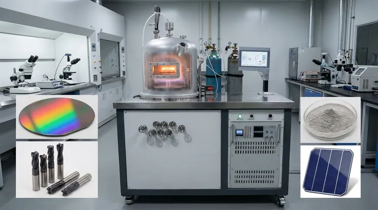
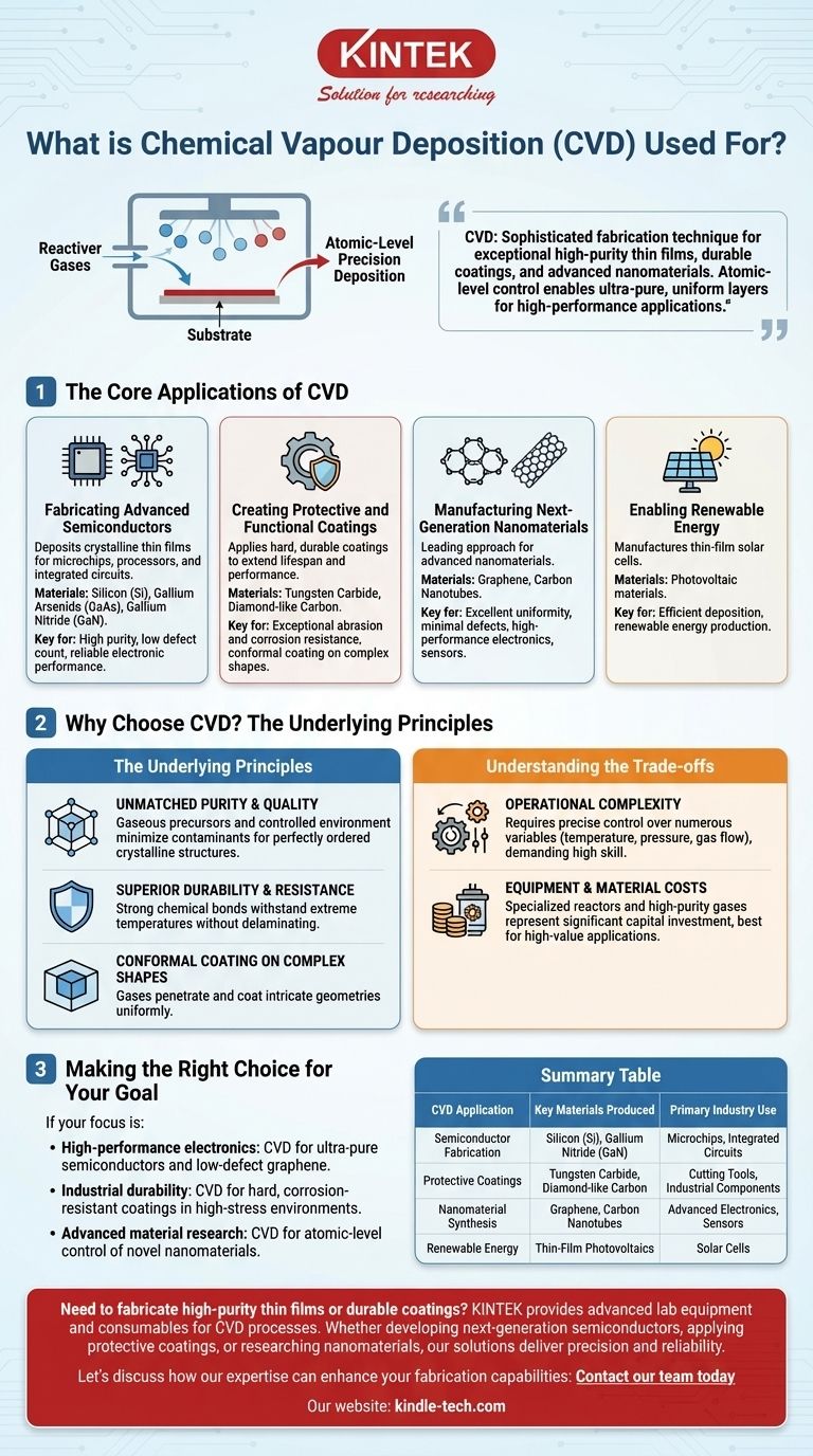
In essence, Chemical Vapor Deposition (CVD) is a sophisticated fabrication technique used to create exceptionally high-purity thin films, durable coatings, and advanced nanomaterials. It is the cornerstone process for manufacturing items like semiconductor wafers for electronics, protective layers on cutting tools, and next-generation materials such as graphene and carbon nanotubes. The method involves introducing reactive gases into a chamber, which then decompose and deposit a solid material layer-by-layer onto a substrate.
The core value of CVD is not just the wide range of materials it can create, but its ability to do so with atomic-level precision. This control enables the fabrication of ultra-pure, uniform, and durable layers that are essential for high-performance electronics, advanced sensors, and industrial components operating in extreme environments.
The Core Applications of CVD
Chemical Vapor Deposition is not a single-use technology; it is a versatile platform that serves several critical industries. Its applications are defined by the unique properties of the materials it can produce.
Fabricating Advanced Semiconductors
CVD is fundamental to the electronics industry. It is used to deposit the crystalline thin films that form the basis of microchips, processors, and other integrated circuits.
This process is ideal for creating monoatomic materials like silicon (Si) and more complex compound semiconductors such as gallium arsenide (GaAs) and gallium nitride (GaN). The high purity and low defect count of CVD-grown films are critical for reliable electronic performance.
Creating Protective and Functional Coatings
In industrial settings, CVD is used to apply hard, durable coatings to tools and components, dramatically increasing their lifespan and performance.
These coatings provide exceptional abrasion and corrosion resistance, making them ideal for cutting tools, bearings, and parts exposed to high-stress environments. The process ensures the coating conforms perfectly even to complex surfaces.
Manufacturing Next-Generation Nanomaterials
CVD has become a leading approach for manufacturing advanced nanomaterials that promise to revolutionize technology.
It is particularly effective for growing high-quality graphene sheets and carbon nanotubes. The precise control offered by CVD yields materials with excellent uniformity and minimal defects, which is crucial for applications in high-performance electronics and advanced sensors.
Enabling Renewable Energy
The technique also plays a role in the production of clean energy.
CVD is used in the manufacture of thin-film solar cells by efficiently depositing photovoltaic materials onto a glass or metal substrate.
Why Choose CVD? The Underlying Principles
The decision to use CVD is driven by its unique advantages in controlling material properties at a fundamental level.
Unmatched Purity and Quality
Because the materials are built up from gaseous precursors in a controlled environment, the resulting films are of exceptionally high purity.
This process minimizes contaminants and allows for the creation of perfectly ordered crystalline structures, which is a non-negotiable requirement for modern semiconductors.
Superior Durability and Resistance
The deposition process forms strong chemical bonds between the coating and the substrate, resulting in a highly durable and adherent layer.
CVD coatings can withstand extreme temperatures and significant temperature variations without delaminating or degrading, making them suitable for the most demanding applications.
Conformal Coating on Complex Shapes
Unlike line-of-sight deposition methods, the gases in a CVD process can penetrate and coat intricate and complex geometries uniformly.
This "conformal coverage" ensures that even the most complex parts receive a consistent, protective layer across their entire surface.
Understanding the Trade-offs
While powerful, CVD is a sophisticated process with specific requirements that make it unsuitable for every application.
Operational Complexity
Achieving high-quality results with CVD requires precise control over numerous variables, including temperature, pressure, gas composition, and flow rates. This means a high level of skill and expertise is required to operate the equipment successfully.
Equipment and Material Costs
The specialized reactors needed for CVD and the required high-purity precursor gases can represent a significant capital investment. This often positions CVD as a solution for high-value applications where performance justifies the cost.
Making the Right Choice for Your Goal
The decision to use Chemical Vapor Deposition should be based on the specific performance requirements of the final product.
- If your primary focus is high-performance electronics: CVD is the industry standard for creating the ultra-pure semiconductor films and low-defect graphene sheets that modern computing relies on.
- If your primary focus is industrial durability: Use CVD to apply exceptionally hard, corrosion-resistant coatings to tools and components that must survive high-stress, high-temperature environments.
- If your primary focus is advanced material research: CVD provides the atomic-level control necessary for reliably fabricating novel nanomaterials like carbon nanotubes, nanowires, and other exotic structures.
Ultimately, CVD is the enabling technology for applications where material quality and performance at the atomic scale are paramount.
Summary Table:
| CVD Application | Key Materials Produced | Primary Industry Use |
|---|---|---|
| Semiconductor Fabrication | Silicon (Si), Gallium Nitride (GaN) | Microchips, Integrated Circuits |
| Protective Coatings | Tungsten Carbide, Diamond-like Carbon | Cutting Tools, Industrial Components |
| Nanomaterial Synthesis | Graphene, Carbon Nanotubes | Advanced Electronics, Sensors |
| Renewable Energy | Thin-Film Photovoltaics | Solar Cells |
Need to fabricate high-purity thin films or durable coatings?
KINTEK specializes in providing advanced lab equipment and consumables for Chemical Vapor Deposition processes. Whether you are developing next-generation semiconductors, applying protective coatings to industrial tools, or researching nanomaterials like graphene, our solutions deliver the precision and reliability your laboratory requires.
Let's discuss how our expertise can enhance your fabrication capabilities: Contact our team today to find the perfect CVD solution for your specific application.
Visual Guide
Related Products
- Chemical Vapor Deposition CVD Equipment System Chamber Slide PECVD Tube Furnace with Liquid Gasifier PECVD Machine
- RF PECVD System Radio Frequency Plasma-Enhanced Chemical Vapor Deposition RF PECVD
- Microwave Plasma Chemical Vapor Deposition MPCVD Machine System Reactor for Lab and Diamond Growth
- Customer Made Versatile CVD Tube Furnace Chemical Vapor Deposition Chamber System Equipment
- 915MHz MPCVD Diamond Machine Microwave Plasma Chemical Vapor Deposition System Reactor
People Also Ask
- How are carbon nanotubes grown? Master Scalable Production with Chemical Vapor Deposition
- What are the core advantages of PE-CVD in OLED encapsulation? Protect Sensitive Layers with Low-Temp Film Deposition
- How expensive is chemical vapor deposition? Understanding the True Cost of High-Performance Coating
- What is plasma enhanced chemical vapor deposition PECVD equipment? A Guide to Low-Temperature Thin Film Deposition
- What are the processes of vapor phase deposition? Understand CVD vs. PVD for Superior Thin Films


