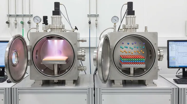
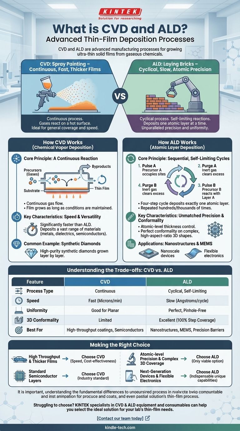
At their core, Chemical Vapor Deposition (CVD) and Atomic Layer Deposition (ALD) are both advanced manufacturing processes used to grow ultra-thin solid films from gaseous chemicals. CVD is a continuous process where gases react on a hot surface, making it relatively fast and ideal for thicker coatings. ALD, a subtype of CVD, is a slower, cyclical process that deposits material one single atomic layer at a time, offering unparalleled precision and uniformity.
The fundamental difference lies in control versus speed. CVD is like spray painting—fast and effective for general coverage. ALD is like meticulously laying bricks one by one—slow, but resulting in a perfect, uniform structure with atomic-level accuracy.
How Chemical Vapor Deposition (CVD) Works
CVD is a foundational technique in materials science and semiconductor manufacturing, valued for its versatility and speed. It is the established workhorse for creating a wide variety of high-performance films.
The Core Principle: A Continuous Reaction
In a CVD process, one or more volatile chemical gases, known as precursors, are introduced into a reaction chamber containing a heated object, or substrate. The heat energizes the precursors, causing them to react and decompose on the substrate's surface, leaving behind a solid thin film. The excess gas and reaction byproducts are then pumped out.
This entire process is continuous, with gas flowing and the film growing as long as the conditions are maintained.
Key Characteristics: Speed and Versatility
Because the deposition happens continuously across the entire surface at once, CVD is significantly faster than ALD. It can be used to deposit a vast range of materials, including metals, dielectrics, and semiconductors.
A Common Example: Synthetic Diamonds
The reference to synthetic diamonds is a classic application of CVD. In this process, a mixture of hydrogen and a carbon-containing gas like methane is heated in a vacuum chamber. This causes carbon atoms to deposit onto a small diamond "seed," slowly growing a larger, high-purity synthetic diamond layer by layer.
How Atomic Layer Deposition (ALD) Works
ALD represents the pinnacle of thin-film control. It was developed to overcome the limitations of CVD in applications demanding absolute precision and the ability to coat highly complex, three-dimensional structures.
The Core Principle: Sequential, Self-Limiting Cycles
Unlike the continuous nature of CVD, ALD is a cyclical process. A single cycle consists of four distinct steps:
- Pulse A: A first precursor gas is pulsed into the chamber. It reacts with the substrate surface until every available reaction site is occupied, forming a single, complete atomic layer. This reaction is self-limiting; no further material can deposit.
- Purge A: The chamber is purged with an inert gas to remove all excess precursor A gas.
- Pulse B: A second precursor gas (the reactant) is pulsed in. It reacts exclusively with the first layer that was just deposited. This reaction is also self-limiting.
- Purge B: The chamber is purged again to remove excess precursor B and any gaseous byproducts.
This four-step cycle deposits exactly one atomic layer and is repeated hundreds or thousands of times to build a film of the desired thickness.
Key Characteristics: Unmatched Precision and Conformality
The self-limiting nature of ALD gives it two critical advantages. First is atomic-level thickness control, as the final film thickness is simply the number of cycles multiplied by the deposition rate per cycle.
Second is perfect conformality. The process can perfectly coat the insides of incredibly deep, narrow trenches and complex 3D shapes because the precursor gases can diffuse into any exposed area before reacting.
Understanding the Trade-offs: CVD vs. ALD
Choosing between these two techniques is a critical engineering decision based on a clear set of trade-offs. There is no universally "better" method; the choice depends entirely on the application's requirements.
Deposition Speed
CVD is dramatically faster than ALD, often by one or two orders of magnitude. For films that are microns thick, CVD is the only practical choice from a throughput perspective.
Film Quality and Uniformity
ALD provides superior, pinhole-free films. Because it builds the material one atomic layer at a time, it produces films with unparalleled uniformity and density. CVD films can have variations in thickness and are more prone to defects.
Conformality on 3D Structures
ALD is the undisputed champion of conformality. It can achieve 100% step coverage on high-aspect-ratio structures, like the deep trenches in DRAM capacitors or the fins of a modern FinFET transistor. CVD struggles to coat such complex topographies uniformly.
Cost and Complexity
CVD is generally cheaper and simpler for a given area. The equipment is more straightforward, and the high speed leads to lower cost per part. ALD tools are more complex due to the precise pulsing and purging requirements, and the slow speed increases the processing time and cost.
Making the Right Choice for Your Application
Your final decision must be guided by the non-negotiable requirements of your project. Balancing performance, cost, and speed is key.
- If your primary focus is high throughput for thicker protective or optical coatings: Choose CVD for its speed and cost-effectiveness.
- If your primary focus is atomic-level precision and perfect coverage on complex nanostructures: ALD is the only viable option.
- If you are fabricating standard semiconductor layers where some thickness variation is acceptable: CVD is often the industry standard.
- If you are developing next-generation transistors, MEMS devices, or moisture barriers for flexible electronics: The unique capabilities of ALD are indispensable.
Ultimately, understanding the fundamental difference between a continuous process and a self-limiting cyclic one empowers you to select the ideal tool for any thin-film challenge.
Summary Table:
| Feature | CVD (Chemical Vapor Deposition) | ALD (Atomic Layer Deposition) |
|---|---|---|
| Process Type | Continuous gas flow | Cyclical, self-limiting pulses |
| Speed | Fast (ideal for thick films) | Slow (atomic layer control) |
| Uniformity | Good for planar surfaces | Perfect, pinhole-free films |
| 3D Conformality | Limited on complex structures | Excellent (100% step coverage) |
| Best For | High-throughput coatings, semiconductors | Nanostructures, MEMS, precision barriers |
Struggling to choose between CVD and ALD for your lab's thin-film needs? KINTEK specializes in providing the right lab equipment and consumables for both CVD and ALD processes. Our experts can help you select the ideal solution for semiconductor manufacturing, MEMS development, or advanced coating applications. Contact our team today to discuss your specific requirements and enhance your research capabilities with precision and efficiency.
Visual Guide
Related Products
- CVD Diamond Dressing Tools for Precision Applications
- Multi Heating Zones CVD Tube Furnace Machine Chemical Vapor Deposition Chamber System Equipment
- CVD Diamond Domes for Industrial and Scientific Applications
- CVD Diamond for Thermal Management Applications
- Chemical Vapor Deposition CVD Equipment System Chamber Slide PECVD Tube Furnace with Liquid Gasifier PECVD Machine
People Also Ask
- Does the chemical vapor deposition be used for diamonds? Yes, for Growing High-Purity Lab Diamonds
- How long does it take to make synthetic diamonds? Discover the 6-8 Week Science Behind Lab-Grown Gems
- What is chemical vapor deposition of diamond? Grow High-Purity Diamonds Atom-by-Atom
- What color diamonds are CVD? Understanding the Process from Brown Tint to Colorless Beauty
- What are the disadvantages of CVD diamonds? Understanding the trade-offs for your purchase.


