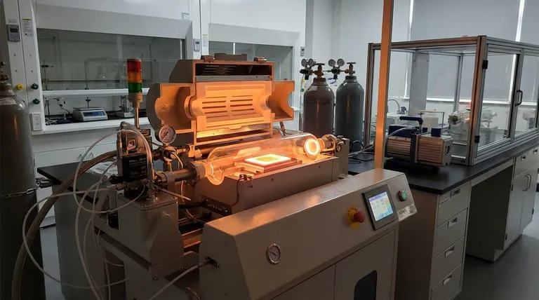
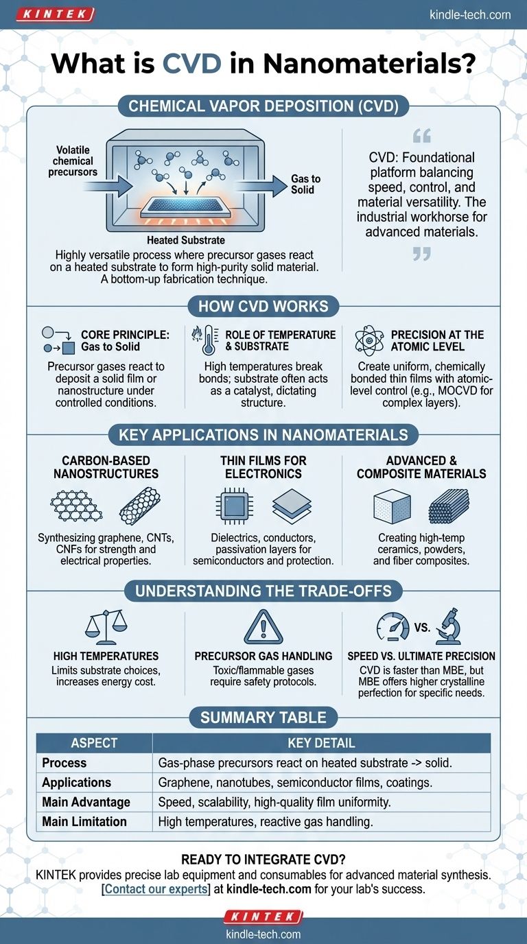
In the context of nanomaterials, CVD stands for Chemical Vapor Deposition. It is a highly versatile process where volatile chemical precursors in a gas phase react or decompose on a heated surface, known as a substrate, to form a high-purity solid material. This bottom-up fabrication technique is fundamental to producing a wide range of nanoscale structures, from single-atom-thick sheets of graphene to complex semiconductor layers.
Chemical Vapor Deposition is not just one technique; it is a foundational platform for manufacturing advanced materials. Its true value lies in its ability to balance speed, control, and material versatility, making it the industrial workhorse for producing many of the most important nanomaterials used today.
How Chemical Vapor Deposition Works
The Core Principle: Gas to Solid
At its heart, CVD is a conversion process. Precursor gases, which contain the atoms of the desired material, are introduced into a reaction chamber.
By carefully controlling conditions like temperature and pressure, these gases are induced to react and deposit a solid film or nanostructure onto a chosen substrate.
The Role of Temperature and Substrate
High temperatures (often several hundred degrees Celsius) provide the necessary energy to break the chemical bonds in the precursor gases.
The substrate is not just a passive surface; it often plays a critical catalytic role in the deposition process and dictates the structure and orientation of the resulting nanomaterial.
Precision at the Atomic Level
While other methods exist, CVD is valued for its ability to create uniform, chemically bonded thin films with atomic-level control over thickness and composition.
Specialized variations, like Metalorganic CVD (MOCVD), allow for the growth of highly complex crystalline layers, which is essential for modern electronics and optoelectronics.
Key Applications in Nanomaterials
Carbon-Based Nanostructures
CVD is the dominant method for synthesizing many revolutionary carbon nanomaterials.
This includes producing large-area, high-quality graphene sheets, as well as carbon nanotubes (CNTs) and carbon nanofibers (CNFs), which are prized for their exceptional strength and electrical properties.
Thin Films for Electronics and Protection
The process is extensively used to deposit a variety of thin films for the semiconductor industry.
These films serve as dielectrics (insulators), conductors, and passivation layers that protect electronic components from the environment. It is also used to create corrosion-resistant and heat-resistant coatings.
Advanced and Composite Materials
Beyond simple films, CVD is used to create complex materials. This includes synthesizing high-temperature ceramics, powders with well-defined particle sizes, and even infiltrating fiber fabrics to create robust fiber composites.
Understanding the Trade-offs
High Temperature Requirements
The high temperatures needed for CVD can limit the types of substrates that can be used, as some materials may melt or deform. This energy consumption also contributes to the overall cost of the process.
Precursor Gas Handling
The chemical precursors used in CVD are often toxic, flammable, or corrosive, requiring sophisticated handling and safety protocols. This can increase the complexity and cost of a CVD setup.
Speed vs. Ultimate Precision
CVD is generally much faster than techniques like Molecular Beam Epitaxy (MBE), which deposits material one atomic layer at a time in an ultra-high vacuum.
However, for applications demanding the absolute highest level of crystalline perfection and interface sharpness, the slower, more controlled nature of MBE may be preferred. CVD offers a powerful balance of speed and high quality, but it is not always the most precise option available.
How to Apply This to Your Project
Choosing a fabrication method depends entirely on your end goal, balancing cost, material requirements, and desired performance.
- If your primary focus is large-scale production of high-quality thin films or carbon nanotubes: CVD is often the most effective and economically viable choice due to its speed and scalability.
- If your primary focus is creating flawless, single-crystal epitaxial layers for high-performance microelectronics: A more specialized and slower method like Molecular Beam Epitaxy (MBE) may be necessary.
- If your primary focus is growing intricate crystalline layers for LEDs or advanced semiconductors: A specialized variant like Metalorganic CVD (MOCVD) will likely be the required tool.
Mastering the principles of CVD is fundamental to leveraging the transformative potential of nanomaterials in nearly every field of modern technology.
Summary Table:
| Aspect | Key Detail |
|---|---|
| Process | Gas-phase precursors react on a heated substrate to form a solid material. |
| Key Applications | Graphene sheets, carbon nanotubes, semiconductor thin films, protective coatings. |
| Main Advantage | Excellent balance of speed, scalability, and high-quality film uniformity. |
| Main Limitation | High temperatures and handling of reactive precursor gases. |
Ready to integrate CVD technology into your lab's workflow? KINTEK specializes in providing the precise lab equipment and consumables needed for advanced material synthesis. Whether you are developing next-generation electronics or high-performance coatings, our expertise supports your innovation from research to production. Contact our experts today to discuss how we can equip your laboratory for success.
Visual Guide
Related Products
- CVD Diamond Dressing Tools for Precision Applications
- Multi Heating Zones CVD Tube Furnace Machine Chemical Vapor Deposition Chamber System Equipment
- CVD Diamond Domes for Industrial and Scientific Applications
- CVD Diamond for Thermal Management Applications
- Chemical Vapor Deposition CVD Equipment System Chamber Slide PECVD Tube Furnace with Liquid Gasifier PECVD Machine
People Also Ask
- Can CVD diamonds change color? No, their color is permanent and stable.
- How long does it take to make synthetic diamonds? Discover the 6-8 Week Science Behind Lab-Grown Gems
- How do CVD diamonds grow? A Step-by-Step Guide to Lab-Grown Diamond Creation
- What color diamonds are CVD? Understanding the Process from Brown Tint to Colorless Beauty
- What is CVD diamond? The Ultimate Guide to Lab-Grown Diamonds and Their Uses


