Chemical Vapor Deposition (CVD) is a foundational bottom-up synthesis method used to create high-purity, high-performance solid materials. In the context of nanomaterials, it involves introducing reactive gases (precursors) into a chamber where they decompose on a heated surface (substrate), depositing a thin film or growing nanostructures like carbon nanotubes or graphene atom by atom.
At its core, CVD is not merely a coating technique; it is a precise fabrication process. Its true value lies in its ability to build atomically precise, chemically bonded nanomaterials from a gaseous state, offering unparalleled control over structure and purity.
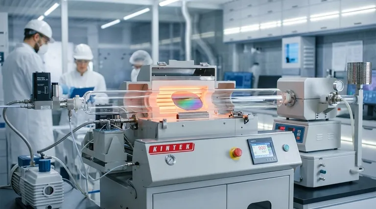
The Core Mechanism: From Gas to Solid
To understand CVD's power, you must first understand its fundamental steps. The process transforms volatile gas molecules into a stable, solid material in a highly controlled environment.
The Role of Precursors and a Substrate
The process begins with two key components: a precursor gas and a substrate. The precursor is a volatile compound that contains the atoms you wish to deposit. The substrate is the surface upon which the new material will be formed.
The Reaction Chamber
These components are placed inside a reaction chamber where conditions like temperature, pressure, and gas flow can be meticulously controlled. This control is essential for determining the final properties of the nanomaterial.
Thermal Decomposition and Deposition
The substrate is heated to a high temperature. When the precursor gas flows over this hot surface, it undergoes thermal decomposition, breaking its chemical bonds. The desired atoms are then "deposited" onto the substrate surface, forming a solid layer.
Building the Nanomaterial
This deposition process can build a uniform thin film across the entire substrate. Alternatively, with the help of a catalyst, it can encourage the growth of specific nanostructures, such as carbon nanotubes or nanofibers.
Removal of Byproducts
The unwanted atoms from the decomposed precursor gas form volatile byproducts. These are simply swept out of the chamber by the continuous gas flow, leaving behind a pure layer of the desired material.
Why CVD is a Dominant Nanofabrication Technique
CVD is not just one method among many; it is a cornerstone of modern materials science and semiconductor manufacturing for several key reasons.
Atomic-Level Precision
Because the material is built atom by atom, CVD allows for exceptional control over thickness, uniformity, and atomic structure. This results in highly ordered, crystalline films with very few defects.
Unmatched Material Versatility
CVD is remarkably flexible. It is used to synthesize a vast range of critical nanomaterials, including:
- Carbon-based materials: Graphene, carbon nanotubes (CNTs), fullerenes, and carbon nanofibers (CNFs).
- Inorganic compounds: Oxides, nitrides (like silicon nitride), and carbides.
- Semiconductor layers: Specialized variants like Metalorganic CVD (MOCVD) are essential for building complex, multi-layered semiconductor wafers.
Purity and Chemical Bonding
The process naturally produces materials with very high chemical purity because the byproducts are efficiently removed. The deposited atoms form strong chemical bonds with the substrate, creating a durable and stable final product.
Understanding the Trade-offs
While powerful, CVD is not a universal solution. A clear understanding of its operational demands is critical for successful implementation.
High Temperature Requirements
Traditional CVD often operates at very high temperatures. This can limit the choice of substrate materials to those that can withstand the heat and contributes to higher energy consumption.
Precursor Handling and Safety
The precursor gases used in CVD can be highly toxic, flammable, or corrosive. This necessitates strict safety protocols, specialized handling equipment, and exhaust gas management, adding to operational complexity and cost.
Process Complexity
Achieving a high-quality, uniform deposition is a delicate balancing act. It requires precise and stable control over multiple variables, including temperature, pressure, gas flow rates, and precursor concentration. This makes process optimization a non-trivial task.
Making the Right Choice for Your Goal
Selecting a synthesis method depends entirely on your end goal. CVD is the superior choice for applications where material quality and structural integrity are paramount.
- If your primary focus is high-purity crystalline structures: CVD is the ideal method for creating materials like single-layer graphene or single-walled CNTs where a flawless atomic lattice is non-negotiable.
- If your primary focus is advanced semiconductor devices: Specialized CVD techniques are the industry standard for growing the complex, epitaxial layers required for modern electronics and optoelectronics.
- If your primary focus is producing robust composite materials: CVD excels at infiltrating fabric or fiber preforms to deposit a functional coating, enhancing the strength and performance of the final composite.
- If your primary focus is rapid or low-cost synthesis for initial research: The high equipment cost and process complexity of CVD may make other methods, like sol-gel or hydrothermal synthesis, a more practical starting point.
By mastering the interplay of gas, heat, and surface, CVD provides a powerful pathway to engineer materials from the atom up.
Summary Table:
| Key Aspect | Description |
|---|---|
| Process | Precursor gases decompose on a heated substrate to deposit a solid material atom by atom. |
| Key Advantages | Atomic-level precision, high material purity, versatility (graphene, CNTs, semiconductors). |
| Key Considerations | High temperatures, requires handling of reactive gases, complex process control. |
| Ideal For | Applications requiring high-purity, crystalline nanomaterials and robust thin films. |
Ready to integrate precise nanomaterial synthesis into your lab's workflow?
KINTEK specializes in providing the advanced lab equipment and consumables you need to leverage techniques like CVD. Our solutions are designed for researchers and engineers focused on developing next-generation materials, from graphene to advanced semiconductors.
We can help you achieve the high-purity, atomically precise results that CVD is renowned for. Contact our experts today to discuss your specific nanomaterials synthesis challenges and goals.
Visual Guide

Related Products
- CVD Diamond Dressing Tools for Precision Applications
- Multi Heating Zones CVD Tube Furnace Machine Chemical Vapor Deposition Chamber System Equipment
- CVD Diamond Domes for Industrial and Scientific Applications
- CVD Diamond for Thermal Management Applications
- Chemical Vapor Deposition CVD Equipment System Chamber Slide PECVD Tube Furnace with Liquid Gasifier PECVD Machine
People Also Ask
- What color diamonds are CVD? Understanding the Process from Brown Tint to Colorless Beauty
- What is chemical vapor deposition of diamond? Grow High-Purity Diamonds Atom-by-Atom
- Can CVD diamonds change color? No, their color is permanent and stable.
- What are the disadvantages of CVD diamonds? Understanding the trade-offs for your purchase.
- How long does it take to make synthetic diamonds? Discover the 6-8 Week Science Behind Lab-Grown Gems


