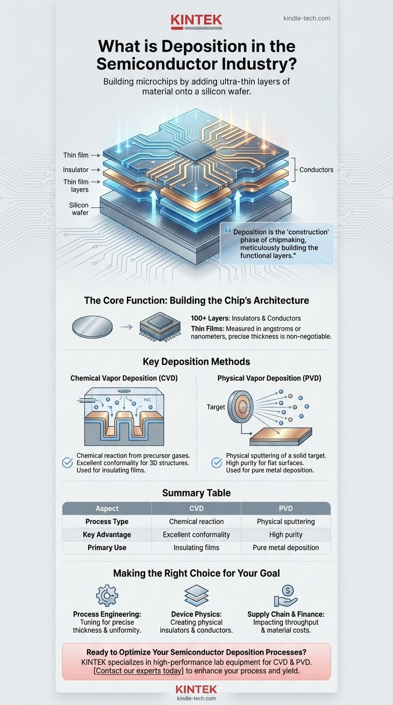
In semiconductor manufacturing, deposition is the fundamental process of building a microchip by adding ultra-thin layers of material onto a silicon wafer. This controlled addition of atomic or molecular films is what creates the essential insulating and conductive structures that form the chip's complex electrical circuits.
The core principle to grasp is that deposition is the "construction" phase of chipmaking. While other steps draw the blueprints (photolithography) or carve away material (etching), deposition is what meticulously builds the functional layers of the integrated circuit.
The Core Function: Building the Chip's Architecture
Deposition is not simply coating a surface; it's a series of highly precise engineering steps that transform a blank silicon wafer into a multi-layered electronic device.
From Bare Silicon to Complex Circuits
A finished microprocessor can have over 100 distinct layers of material stacked on top of one another. Deposition is the process responsible for creating each of these layers.
This includes adding insulating layers (like silicon dioxide) to prevent electrical current from leaking and conductive layers (like copper or tungsten) to form the wires and transistors that carry signals.
The Concept of Thin Films
The layers added during deposition are known as thin films. Their thickness is measured in angstroms or nanometers, often just a few dozen to a few hundred atoms thick.
The precise thickness, purity, and structural quality of each thin film are non-negotiable. Even a minor deviation can drastically alter the electrical properties of the final device, rendering the entire chip useless.
Key Deposition Methods
The choice of deposition method depends entirely on the material being deposited and its purpose within the chip's architecture. The two most fundamental categories are Chemical Vapor Deposition and Physical Vapor Deposition.
Chemical Vapor Deposition (CVD)
CVD is the most widely used deposition technology. It works by introducing one or more precursor gases into a reaction chamber containing the silicon wafers.
These gases react chemically, and a solid byproduct of that reaction is "deposited" as a uniform thin film on the wafer surface. Think of it as a controlled chemical reaction where the solid output forms a new layer on the chip.
CVD is essential for creating high-quality insulating films and various metallic layers.
Physical Vapor Deposition (PVD)
PVD, in contrast, is a mechanical or electromechanical process. In a common PVD technique called "sputtering," a solid target of the desired material is bombarded with high-energy ions.
This bombardment knocks atoms loose from the target, which then travel through a vacuum and coat the wafer. Imagine it as a form of atomic-level spray painting. PVD is excellent for depositing pure metals.
Understanding the Trade-offs
Neither method is universally superior; they are chosen to solve specific geometric and material challenges presented by the chip's design.
The Advantage of CVD: Conformality
CVD's primary advantage is its excellent conformality. Because the deposition happens from a reactive gas, it can evenly coat all surfaces of a complex, three-dimensional structure, including the bottom and sidewalls of deep trenches.
The Advantage of PVD: Line-of-Sight
PVD is a line-of-sight process. The sputtered atoms travel in a relatively straight line, making it difficult to coat the vertical sidewalls of a deep trench. Its strength lies in depositing very pure materials onto flatter surfaces.
The Choice Depends on the Layer's Function
Engineers choose the method based on the need. To create a perfect insulating barrier inside a deep, narrow transistor gate, the superior conformality of CVD is required. To lay down a primary metal interconnect on a relatively flat plane, the speed and purity of PVD might be the optimal choice.
Making the Right Choice for Your Goal
How you view deposition depends on your role in the semiconductor ecosystem. Understanding its function is key to understanding the entire manufacturing flow.
- If your primary focus is process engineering: Your challenge is selecting and tuning the right deposition method (CVD, PVD, ALD, etc.) to achieve the precise film thickness, uniformity, and material properties required for a specific layer.
- If your primary focus is device physics: You see deposition as the tool that creates the physical insulators and conductors whose properties directly determine the transistor's electrical performance and reliability.
- If your primary focus is supply chain or finance: Deposition represents a major capital and operational expense, where the choice of technology directly impacts factory throughput, material costs, and equipment uptime.
Ultimately, understanding deposition is understanding how a modern microchip is constructed from the atoms up.
Summary Table:
| Aspect | Chemical Vapor Deposition (CVD) | Physical Vapor Deposition (PVD) |
|---|---|---|
| Process Type | Chemical reaction from precursor gases | Physical sputtering of a solid target |
| Key Advantage | Excellent conformality for 3D structures | High purity for flat surfaces |
| Primary Use | Insulating films, complex metallic layers | Pure metal deposition |
Ready to Optimize Your Semiconductor Deposition Processes?
KINTEK specializes in providing high-performance lab equipment and consumables for semiconductor R&D and manufacturing. Whether you are developing next-generation CVD techniques or require reliable PVD solutions, our expertise ensures you achieve the precise film thickness, uniformity, and material purity critical for your microchips.
Contact our experts today via our Contact Form to discuss how our tailored solutions can enhance your deposition process, improve yield, and accelerate your time-to-market.
Visual Guide
Related Products
- Chemical Vapor Deposition CVD Equipment System Chamber Slide PECVD Tube Furnace with Liquid Gasifier PECVD Machine
- 915MHz MPCVD Diamond Machine Microwave Plasma Chemical Vapor Deposition System Reactor
- Customer Made Versatile CVD Tube Furnace Chemical Vapor Deposition Chamber System Equipment
- HFCVD Machine System Equipment for Drawing Die Nano-Diamond Coating
- Split Chamber CVD Tube Furnace with Vacuum Station Chemical Vapor Deposition System Equipment Machine
People Also Ask
- What happens during deposition chemistry? Building Thin Films from Gaseous Precursors
- How expensive is chemical vapor deposition? Understanding the True Cost of High-Performance Coating
- What are the processes of vapor phase deposition? Understand CVD vs. PVD for Superior Thin Films
- What are the core advantages of PE-CVD in OLED encapsulation? Protect Sensitive Layers with Low-Temp Film Deposition
- How are carbon nanotubes grown? Master Scalable Production with Chemical Vapor Deposition


