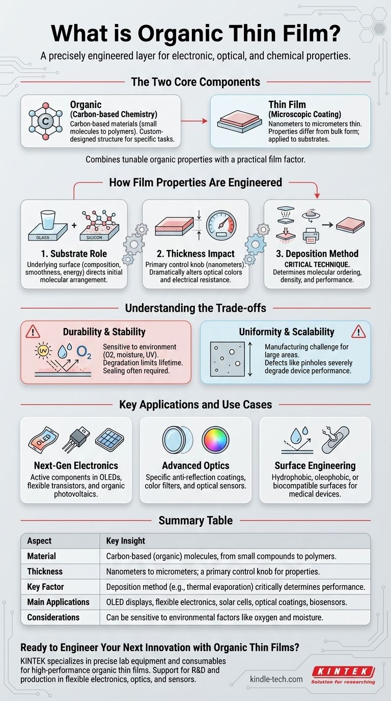
At its core, an organic thin film is an extremely thin layer of a carbon-based material intentionally applied to a surface, or substrate. Think of it not as a simple coating, but as a precisely engineered layer, often just a few molecules thick, designed to give that surface entirely new electronic, optical, or chemical properties.
The central concept to grasp is that organic thin films combine the highly tunable and diverse properties of organic molecules with the practical form factor of a microscopic coating, enabling technologies from flexible displays to advanced biosensors.

The Two Core Components
The term "organic thin film" describes two distinct but inseparable characteristics: the material it's made from and the form it takes. Understanding both is key to understanding its function.
Defining "Organic" in this Context
The word "organic" here refers to materials based on carbon chemistry. This includes a vast range of compounds, from small molecules to long-chain polymers.
These are not inorganic materials like metals or ceramics. Instead, their properties are derived from the structure and electronic configuration of the molecules themselves, which can be custom-designed for specific tasks.
Understanding the "Thin Film" Form
A "thin film" is a layer of material ranging from nanometers to several micrometers in thickness. This microscopic scale is critical.
At this thickness, the properties of the material can be dramatically different from its bulk form. The film format makes it possible to apply these properties to a substrate like glass, silicon, or flexible plastic.
How Film Properties Are Engineered
The final characteristics of an organic thin film are not accidental. They are the result of a carefully controlled engineering process where several factors must be managed to achieve the desired outcome.
The Critical Role of the Substrate
The underlying surface, or substrate, is an active participant in the film's creation. Its own properties—such as its chemical composition, smoothness, and energy—dictate how the first layers of organic molecules arrange themselves.
This initial arrangement can influence the structure of the entire film, directly impacting its final electronic or optical performance.
The Impact of Film Thickness
As mentioned in the references, thickness is a primary control knob for tuning a film's properties. In optical applications, changing the thickness by just a few nanometers can alter which colors of light it reflects or transmits.
In electronics, thickness directly influences factors like electrical resistance and capacitance, which are fundamental to device performance.
The Influence of Deposition Method
How the film is applied, known as the deposition technique, is arguably the most critical factor. Methods like thermal evaporation, spin-coating, or printing determine the molecular ordering and density of the film.
A poorly controlled deposition can result in defects and inconsistent performance, while a precise method can create highly ordered, high-performance films.
Understanding the Trade-offs
While powerful, organic thin films are not a universal solution. Their unique nature comes with specific challenges and limitations that must be considered.
Durability and Stability
Many organic materials are sensitive to their environment. Exposure to oxygen, moisture, and ultraviolet (UV) light can degrade the molecules over time, altering the film's properties and limiting its operational lifetime.
This is a primary reason why devices like OLED screens are meticulously sealed to protect the organic layers from the ambient environment.
Uniformity and Scalability
Creating a perfectly uniform film, with the same thickness and structure over a large area, is a significant manufacturing challenge.
Defects like pinholes or regions of different thickness can severely degrade the performance of a device, especially for applications like large-screen displays or solar panels.
Key Applications and Use Cases
The unique properties of organic thin films make them essential for several modern technologies. Your interest in them likely aligns with one of these goals.
- If your primary focus is next-generation electronics: These films are the active components in OLED displays, flexible transistors, and organic photovoltaic (solar) cells.
- If your primary focus is advanced optics: They are used to create highly specific anti-reflection coatings, color filters, and specialized optical sensors.
- If your primary focus is surface engineering: Organic thin films can be used to make surfaces hydrophobic (water-repellent), oleophobic (oil-repellent), or biocompatible for medical implants.
Ultimately, organic thin films represent a powerful platform for engineering material properties at the molecular level and applying them to real-world surfaces.
Summary Table:
| Aspect | Key Insight |
|---|---|
| Material | Carbon-based (organic) molecules, from small compounds to polymers. |
| Thickness | Nanometers to micrometers; a primary control knob for properties. |
| Key Factor | Deposition method (e.g., thermal evaporation) critically determines performance. |
| Main Applications | OLED displays, flexible electronics, solar cells, optical coatings, biosensors. |
| Considerations | Can be sensitive to environmental factors like oxygen and moisture. |
Ready to Engineer Your Next Innovation with Organic Thin Films?
At KINTEK, we specialize in the precise lab equipment and consumables needed for developing and applying high-performance organic thin films. Whether you are creating flexible electronics, advanced optical coatings, or specialized sensors, our solutions support your R&D and production.
Contact our experts today to discuss how we can help you achieve superior film uniformity, performance, and scalability for your specific application.
Visual Guide
Related Products
- Laboratory CVD Boron Doped Diamond Materials
- Battery Lab Equipment 304 Stainless Steel Strip Foil 20um Thick for Battery Test
- Professional Cutting Tools for Carbon Paper Cloth Diaphragm Copper Aluminum Foil and More
- Thin-Layer Spectral Electrolysis Electrochemical Cell
- Float Soda-Lime Optical Glass for Laboratory Use
People Also Ask
- How much cheaper are CVD diamonds? Save 20-30% on a Genuine Diamond
- Do CVD diamonds pass diamond tester? Yes, they are real diamonds.
- What is the purpose of adding a boron source in CVD diamond growth? Master P-Type Semiconductor Conductivity
- Are CVD diamonds good? Real Diamonds with Ethical Origins & Better Value
- What are the applications of CVD diamonds? From Jewelry to High-Tech Tools