At its core, plasma magnetron sputtering is a sophisticated coating technique used to deposit exceptionally thin and uniform films of material onto a surface. It is a physical vapor deposition (PVD) process that operates in a high vacuum, using a magnetically-confined plasma to bombard a source material. This bombardment ejects atoms from the source, which then travel and condense on a substrate, forming the desired coating.
The defining characteristic of magnetron sputtering is its strategic use of a magnetic field. While the basic process involves using plasma to knock atoms off a target, the magnetron's field traps electrons, creating a highly dense and efficient plasma that enables faster, more controlled deposition at lower pressures.
The Core Mechanism: A Controlled Atomic Collision
To understand magnetron sputtering, it's best to break it down into a sequence of controlled physical events happening inside a vacuum chamber.
Step 1: Creating the Environment
The entire process must occur in a high vacuum chamber. This removes air and other contaminants that could interfere with the coating process. An inert gas, most commonly argon, is then introduced at a very low pressure.
Step 2: Igniting the Plasma
A high voltage is applied across the chamber, creating a strong electric field between two electrodes: the anode and the cathode. The cathode is also the target, which is made from the material you wish to deposit. This electric field energizes the argon gas, stripping electrons from the argon atoms and creating a glowing, ionized gas known as a plasma—a mix of positive argon ions and free electrons.
Step 3: The Sputtering Event
The positively charged argon ions are accelerated by the electric field and smash into the negatively charged target. This high-energy bombardment physically knocks atoms loose from the target's surface. This ejection of atoms is the sputtering process.
Step 4: Thin-Film Deposition
The ejected atoms from the target travel through the vacuum chamber and land on the substrate (the object being coated). As these atoms accumulate, they condense and build up, layer by layer, to form a dense, uniform, and highly adherent thin film.
The "Magnetron" Advantage: Why the Magnetic Field is Critical
Without a magnetic field, the process described above would be simple "diode sputtering," which is slow and inefficient. The addition of a magnetron—a specific arrangement of magnets behind the target—revolutionizes the process.
Enhancing Plasma Density
The key is the magnetic field's effect on the free electrons in the plasma. The magnets trap these light electrons in a spiral path directly in front of the target. By confining them, the probability that an electron will collide with and ionize a neutral argon atom increases dramatically.
Boosting Efficiency and Speed
This increased ionization creates a much denser, more intense plasma concentrated near the target. A denser plasma means more argon ions are available to bombard the target, which significantly increases the sputtering rate and speeds up the entire coating process.
Enabling Lower Pressures
Because the magnetic field makes the ionization process so efficient, magnetron sputtering can operate at much lower gas pressures. A lower pressure means fewer gas atoms are in the path of the sputtered atoms traveling to the substrate, resulting in a cleaner, higher-purity film.
Understanding the Trade-offs
Like any advanced process, magnetron sputtering has distinct benefits and inherent limitations that make it suitable for specific applications.
Benefit: Unmatched Material Versatility
The process is purely physical, not thermal. This means you can sputter virtually any material—including metals, alloys, and ceramics—without having to melt or evaporate it. This is a major advantage for depositing materials with extremely high melting points.
Benefit: Superior Film Quality
Magnetron sputtering produces films that are incredibly dense, uniform, and have excellent adhesion to the substrate. This results in highly durable and high-performance coatings.
Limitation: Line-of-Sight Deposition
The sputtered atoms travel in a straight line from the target to the substrate. This makes it challenging to uniformly coat complex, three-dimensional shapes with hidden surfaces or deep trenches.
Limitation: System Complexity
The required equipment—a high vacuum chamber, high-voltage power supplies, precisely controlled gas inlets, and strong magnetic arrays—is complex and expensive. The process requires significant expertise to operate correctly.
How to Apply This to Your Project
Deciding if magnetron sputtering is the right choice depends entirely on your specific material and performance requirements.
- If your primary focus is high-performance optical or electronic coatings: This method's ability to create exceptionally pure, dense, and uniform films is ideal for applications like anti-reflective lenses, semiconductors, or sensors.
- If your primary focus is durable and functional surface coatings: For adding wear resistance, corrosion protection, or specific conductive properties to tools or components, this process provides superior adhesion and durability.
- If your primary focus is coating heat-sensitive substrates: Because the process does not require melting the source material, it is perfect for depositing high-melting-point materials onto substrates like plastics that cannot withstand high temperatures.
Ultimately, understanding the interplay of plasma physics and magnetic control is the key to leveraging magnetron sputtering for advanced material engineering.
Summary Table:
| Aspect | Key Detail |
|---|---|
| Process Type | Physical Vapor Deposition (PVD) |
| Core Mechanism | Magnetic field traps electrons to create a dense plasma that sputters target atoms onto a substrate. |
| Primary Use | Depositing thin, uniform, and highly adherent films of metals, alloys, and ceramics. |
| Key Advantage | High film quality, material versatility, and efficient deposition at lower pressures. |
| Main Limitation | Line-of-sight deposition can make coating complex 3D shapes challenging. |
Need a high-performance coating solution for your lab's research or production?
The advanced control and superior film quality of magnetron sputtering can be the key to your project's success. At KINTEK, we specialize in providing state-of-the-art lab equipment, including sputtering systems, to meet the precise needs of laboratories developing next-generation optics, semiconductors, and durable surface coatings.
Let our experts help you select the right equipment to achieve exceptional thin-film results. Contact our team today to discuss your specific application and how we can support your goals.
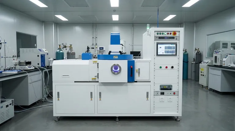
Visual Guide

Related Products
- Spark Plasma Sintering Furnace SPS Furnace
- Chemical Vapor Deposition CVD Equipment System Chamber Slide PECVD Tube Furnace with Liquid Gasifier PECVD Machine
- RF PECVD System Radio Frequency Plasma-Enhanced Chemical Vapor Deposition RF PECVD
- Microwave Plasma Chemical Vapor Deposition MPCVD Machine System Reactor for Lab and Diamond Growth
- 915MHz MPCVD Diamond Machine Microwave Plasma Chemical Vapor Deposition System Reactor
People Also Ask
- What are the advantages of CAMI/SPS for W-Cu composite preparation? Reduce cycles from hours to seconds.
- Why are Spark Plasma Sintering (SPS) furnaces or hot presses utilized in the preparation of Li3PS4 solid electrolytes?
- What is the mechanism of SPS process? A Deep Dive into Rapid, Low-Temperature Sintering
- What is the process fundamentals of spark plasma sintering? Achieve Rapid, High-Density Material Consolidation
- What is the pressure for spark plasma sintering? A Guide to Optimizing SPS Parameters


