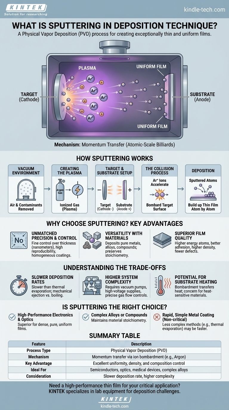
At its core, sputtering is a physical vapor deposition (PVD) technique used to create exceptionally thin and uniform films of material. In this process, a source material, known as the target, is bombarded with high-energy ions inside a vacuum chamber. This atomic-scale collision physically knocks off, or "sputters," atoms from the target, which then travel and deposit onto a component, called the substrate, forming a precise coating.
Sputtering is not a melting or evaporation process; it is a momentum-transfer mechanism, like a microscopic game of billiards. This physical "knock-off" approach gives engineers precise control over film thickness, composition, and uniformity, making it a cornerstone of modern high-technology manufacturing.
How Sputtering Works: An Atomic-Scale Billiard Game
The sputtering process is a highly controlled sequence of events that takes place in a specialized vacuum chamber. Each step is critical for achieving a high-quality, uniform thin film.
The Vacuum Environment
First, the entire process must occur in a vacuum. Air is pumped out of the chamber to remove contaminants like oxygen and water vapor that could react with the sputtered atoms and compromise the purity of the final film.
Creating the Plasma
An inert gas, most commonly argon, is introduced into the chamber at a very low pressure. A strong electric field is then applied. This field energizes free electrons, which collide with the argon atoms, stripping away an electron and creating positively charged argon ions. This energized, ionized gas is known as a plasma.
The Target and Substrate Setup
Inside the chamber, the target—the material you want to deposit—is set up as a negatively charged cathode. The substrate—the object you want to coat—is positioned to face the target and typically acts as the positively charged anode.
The Collision Process
The positively charged argon ions from the plasma are forcefully accelerated towards the negatively charged target. They bombard the target surface with significant kinetic energy.
Deposition onto the Substrate
This high-energy impact has enough force to dislodge atoms from the target material, ejecting them into the vacuum chamber. These sputtered atoms travel in straight lines until they strike the substrate, gradually building up a thin, uniform film atom by atom.
Why Choose Sputtering? Key Advantages
Sputtering is widely used in demanding industries like semiconductors, optics, and medical devices for several key reasons.
Unmatched Precision and Control
The process allows for exceptionally fine control over the film's thickness, down to the scale of nanometers. This results in highly reproducible and homogeneously distributed coatings, which is critical for complex devices.
Versatility with Materials
Sputtering can deposit a vast range of materials, including pure metals, alloys, and compounds like oxides and nitrides. A key advantage is that it can deposit alloys while preserving their original composition, which is difficult with heat-based evaporation methods.
Superior Film Quality
The sputtered atoms arrive at the substrate with higher energy than in thermal evaporation. This often results in films with better adhesion, higher density, and fewer defects, leading to more durable and reliable coatings for applications like cutting tools and anti-reflective glass.
Understanding the Trade-offs
While powerful, sputtering is not the universal solution for every coating need. It is essential to understand its limitations.
Slower Deposition Rates
Compared to a simpler method like thermal evaporation, sputtering is generally a slower process. The mechanical nature of ejecting atoms one by one is less rapid than boiling off material from a source.
Higher System Complexity
Sputtering systems are sophisticated machines requiring vacuum pumps, high-voltage power supplies, and precise gas flow controllers. This complexity increases both the initial investment and the operational expertise required.
Potential for Substrate Heating
The constant bombardment of energetic particles can transfer a significant amount of heat to the substrate. While often manageable, this can be a concern when coating heat-sensitive materials like certain plastics or biological samples.
Is Sputtering the Right Choice for Your Application?
Choosing a deposition method depends entirely on the technical requirements of the final product.
- If your primary focus is high-performance electronics or optical coatings: Sputtering is the superior choice for its ability to create dense, pure, and extremely uniform films of complex materials.
- If your primary focus is depositing complex alloys or compounds: Sputtering excels because it maintains the material's stoichiometry (the original ratio of elements) from target to substrate.
- If your primary focus is rapid, simple metal coating for a non-critical surface: A less complex method like thermal evaporation might be a more cost-effective and faster solution.
Ultimately, selecting sputtering is a decision for precision and quality over speed and simplicity.
Summary Table:
| Feature | Description |
|---|---|
| Process Type | Physical Vapor Deposition (PVD) |
| Mechanism | Momentum transfer via ion bombardment (e.g., Argon) |
| Key Advantage | Excellent film uniformity, density, and material composition control |
| Ideal For | Semiconductors, optics, medical devices, complex alloys |
| Consideration | Slower deposition rate and higher system complexity than some methods |
Need a high-performance thin film for your critical application?
Sputtering delivers the precision, uniformity, and material integrity required for advanced manufacturing in semiconductors, optics, and medical devices. The experts at KINTEK specialize in providing the right lab equipment and consumables to meet your specific deposition challenges.
Contact KINTEK today to discuss how our solutions can enhance your laboratory's capabilities and ensure the quality of your coatings.
Visual Guide
Related Products
- Chemical Vapor Deposition CVD Equipment System Chamber Slide PECVD Tube Furnace with Liquid Gasifier PECVD Machine
- Customer Made Versatile CVD Tube Furnace Chemical Vapor Deposition Chamber System Equipment
- HFCVD Machine System Equipment for Drawing Die Nano-Diamond Coating
- RF PECVD System Radio Frequency Plasma-Enhanced Chemical Vapor Deposition RF PECVD
- 915MHz MPCVD Diamond Machine Microwave Plasma Chemical Vapor Deposition System Reactor
People Also Ask
- What are the processes of vapor phase deposition? Understand CVD vs. PVD for Superior Thin Films
- What is plasma enhanced chemical vapor deposition PECVD equipment? A Guide to Low-Temperature Thin Film Deposition
- What are the advantages of chemical vapor deposition? Achieve Superior Thin Films for Your Lab
- How are carbon nanotubes grown? Master Scalable Production with Chemical Vapor Deposition
- What are the core advantages of PE-CVD in OLED encapsulation? Protect Sensitive Layers with Low-Temp Film Deposition


