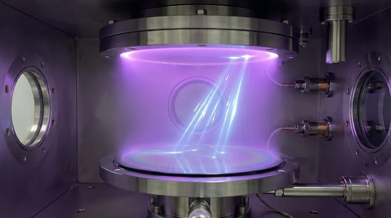
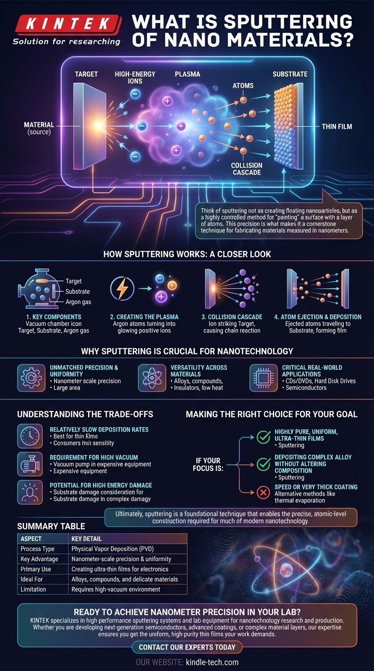
At its core, sputtering is a physical process used to create nanomaterials in the form of ultra-thin films. It works by bombarding a source material (the "target") with high-energy ions, which act like atomic-scale sandblasters. This collision knocks individual atoms loose from the target, which then travel and deposit onto a nearby surface (the "substrate"), building up a new layer one atom at a time.
Think of sputtering not as creating floating nanoparticles, but as a highly controlled method for "painting" a surface with a layer of atoms. This precision is what makes it a cornerstone technique for fabricating materials measured in nanometers.
How Sputtering Works: A Closer Look
Sputtering is a physical vapor deposition (PVD) method that takes place inside a high-vacuum chamber. The mechanism relies on momentum transfer, much like a game of atomic billiards.
The Key Components
The process begins with three essential elements inside a vacuum chamber: a target made of the material you want to deposit, a substrate which is the item you want to coat, and an inert gas like Argon.
Creating the Plasma
A high voltage is applied, which strips electrons from the Argon gas atoms and creates a plasma—a cloud of high-energy positive ions. These ions are then accelerated toward the negatively charged target material.
The Collision Cascade
When a high-energy ion strikes the target, it transfers its momentum to the target's atoms. This initial impact sets off a chain reaction, or collision cascade, near the surface.
Atom Ejection and Deposition
If an atom on the surface of the target receives enough energy from this cascade to overcome its own atomic bonding energy, it is ejected, or "sputtered". This free atom then travels through the vacuum and condenses onto the substrate, forming a thin, uniform film.
Why Sputtering is Crucial for Nanotechnology
Sputtering isn't just one method among many; its unique characteristics make it indispensable for creating the complex, layered structures found in modern electronics and advanced materials.
Unmatched Precision and Uniformity
The primary advantage of sputtering is its control. Because atoms are dislodged physically and predictably, the process can create films with nanometer-scale precision and exceptional uniformity over large areas.
Versatility Across Materials
Unlike methods that rely on melting or evaporation, sputtering can be used with a vast range of materials. It works exceptionally well for depositing alloys, compounds, and insulators whose composition would be altered by high heat.
Critical Real-World Applications
This technique is fundamental to manufacturing many devices we use daily. It's used to deposit the ultra-thin conductive and insulating layers in semiconductor chips, the reflective layers on CDs and DVDs, and the magnetic layers on hard disk drives.
Understanding the Trade-offs
No technique is perfect. While powerful, sputtering has practical limitations that are important to understand.
Relatively Slow Deposition Rates
Compared to some chemical deposition methods, sputtering can be a slow process. It is best suited for creating very thin films (nanometers to a few micrometers) and can be inefficient for applications requiring thick coatings.
Requirement for High Vacuum
The entire process must occur in a high-vacuum environment to prevent sputtered atoms from colliding with air molecules. This necessitates complex and expensive vacuum chamber equipment.
Potential for High Energy Damage
The bombardment of high-energy ions can sometimes impart unwanted stress or minor damage to the substrate. This is a key consideration when working with extremely delicate or sensitive materials.
Making the Right Choice for Your Goal
Selecting a fabrication method depends entirely on your project's specific requirements for precision, material, and efficiency.
- If your primary focus is creating highly pure, uniform, and ultra-thin films: Sputtering is an industry-standard choice for its exceptional control over thickness and composition.
- If your primary focus is depositing a complex alloy without altering its composition: Sputtering is superior to heat-based methods because it physically ejects atoms, preserving the source material's stoichiometry.
- If your primary focus is speed or applying a very thick coating: You may want to investigate alternative methods like thermal evaporation or electroplating, which can offer higher deposition rates.
Ultimately, sputtering is a foundational technique that enables the precise, atomic-level construction required for much of modern nanotechnology.
Summary Table:
| Aspect | Key Detail |
|---|---|
| Process Type | Physical Vapor Deposition (PVD) |
| Key Advantage | Nanometer-scale precision & uniformity |
| Primary Use | Creating ultra-thin films for electronics |
| Ideal For | Alloys, compounds, and delicate materials |
| Limitation | Requires high-vacuum environment |
Ready to achieve nanometer precision in your lab?
KINTEK specializes in high-performance sputtering systems and lab equipment for nanotechnology research and production. Whether you are developing next-generation semiconductors, advanced coatings, or complex material layers, our expertise ensures you get the uniform, high-purity thin films your work demands.
Contact our experts today to discuss your specific needs and discover the right sputtering solution for your laboratory.
Visual Guide
Related Products
- Spark Plasma Sintering Furnace SPS Furnace
- Vacuum Induction Melting Spinning System Arc Melting Furnace
- Chemical Vapor Deposition CVD Equipment System Chamber Slide PECVD Tube Furnace with Liquid Gasifier PECVD Machine
- Customer Made Versatile CVD Tube Furnace Chemical Vapor Deposition Chamber System Equipment
People Also Ask
- What is SPS sintering method? A Guide to High-Speed, High-Performance Material Fabrication
- What is the mechanism of SPS process? A Deep Dive into Rapid, Low-Temperature Sintering
- What is the pressure for spark plasma sintering? A Guide to Optimizing SPS Parameters
- Why are Spark Plasma Sintering (SPS) furnaces or hot presses utilized in the preparation of Li3PS4 solid electrolytes?
- What is the difference between spark plasma sintering and flash sintering? A Guide to Advanced Sintering Methods


