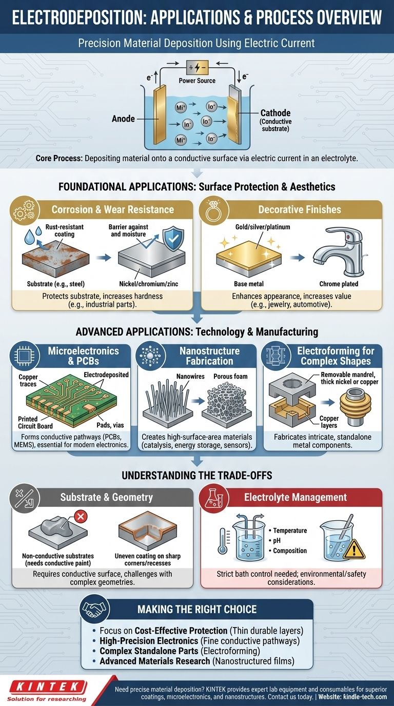
In short, electrodeposition is a process for precisely depositing a material onto a conductive surface using an electric current. This method, also known as electroplating, involves passing current through a chemical solution (electrolyte), causing dissolved metal ions to form a solid, thin film on an object. It's used to create everything from protective coatings on industrial parts to the intricate copper pathways inside electronic devices.
Electrodeposition is far more than a simple coating technique. Its core value lies in its exceptional control over material thickness and structure, enabling the fabrication of everything from corrosion-resistant surfaces to complex, high-performance components at the micro and nanoscale.
Foundational Applications: Surface Protection and Aesthetics
The most common applications of electrodeposition are focused on enhancing the surface of an existing object. This is a cost-effective way to give a bulk material properties it doesn't naturally possess.
Corrosion and Wear Resistance
A primary industrial use is to protect an underlying material, known as the substrate. A thin, non-reactive layer of a metal like nickel, chromium, or zinc can be deposited onto a cheaper or more vulnerable material, such as steel.
This coating acts as a physical barrier, preventing oxygen and moisture from reaching the substrate and causing rust or corrosion. It also provides a harder surface that resists scratching and wear.
Decorative Finishes
Electrodeposition is the cornerstone of creating attractive, high-value finishes. A thin layer of a precious metal like gold, silver, or platinum can be plated onto a less expensive base metal for jewelry.
Similarly, the bright, reflective finish on automotive parts, faucets, and fixtures is often created by electrodepositing a layer of chromium, a process commonly known as chrome plating.
Advanced Applications in Technology and Manufacturing
Beyond simple coatings, electrodeposition is a critical fabrication tool for high-technology industries. Its precision allows for the creation of functional structures, not just surface layers.
Microelectronics and PCBs
The creation of Printed Circuit Boards (PCBs) relies heavily on electrodepositing copper. This process forms the conductive traces, pads, and vias that connect all the electronic components on the board.
The method's ability to deposit pure, uniform layers of copper is essential for the reliability and performance of modern electronics, including micro-electro-mechanical systems (MEMS).
Nanostructure Fabrication
As mentioned in the references, this technique can create nanostructured films. By carefully controlling the electrodeposition parameters, it's possible to grow materials with unique nanoscale textures, such as nanowires or porous foams.
These structures have an incredibly high surface area, making them ideal for applications in catalysis (using platinum) or energy storage. The unique structure can also produce specific optical or magnetic properties for sensors and other advanced devices.
Electroforming for Complex Shapes
Electroforming uses the same principle but takes it a step further. Instead of a thin coating, a thick, structurally independent layer of metal (often nickel or copper) is deposited onto a removable mold or mandrel.
Once the desired thickness is reached, the mandrel is dissolved or removed, leaving a standalone, seamless metal part. This process is excellent for creating complex, hollow, or intricate shapes that would be difficult or impossible to machine, such as waveguides, bellows, and high-precision nozzles.
Understanding the Trade-offs
While powerful, electrodeposition is not a universal solution. Understanding its limitations is key to applying it successfully.
Substrate and Geometry Limitations
The most fundamental requirement is that the substrate must be electrically conductive. While non-conductive materials like plastic can be plated after being coated with a conductive paint, this adds complexity and cost.
Furthermore, achieving a perfectly uniform coating on parts with sharp corners, deep recesses, or complex geometries is challenging. The electric field tends to concentrate on sharp edges, leading to thicker deposits there and thinner deposits in recessed areas.
Electrolyte Management
The chemical bath, or electrolyte, is the heart of the process and requires strict control. Its temperature, pH, and chemical composition must be continuously monitored and maintained to ensure consistent results.
Impurities in the bath can ruin the quality of the deposited layer. Additionally, the handling and disposal of these chemical solutions present significant environmental and safety considerations.
Making the Right Choice for Your Goal
To apply this method effectively, match its capabilities to your specific objective.
- If your primary focus is cost-effective surface protection: Use electrodeposition to apply thin, durable layers like nickel, zinc, or chromium onto steel for industrial-scale corrosion and wear resistance.
- If your primary focus is high-precision electronics: Leverage its ability to create fine, high-purity conductive pathways for PCBs and integrated circuits.
- If your primary focus is creating complex, standalone metal parts: Consider electroforming as a method to replicate intricate shapes that are difficult to machine.
- If your primary focus is advanced materials research: Explore its capability to create nanostructured films with unique catalytic, optical, or magnetic properties.
Ultimately, electrodeposition provides a uniquely versatile and scalable tool for engineering materials from the surface up.
Summary Table:
| Application Area | Key Function | Common Materials |
|---|---|---|
| Surface Protection | Corrosion & wear resistance | Nickel, Chromium, Zinc |
| Decorative Finishes | Aesthetic enhancement | Gold, Silver, Platinum |
| Microelectronics | Conductive pathway creation | Copper |
| Nanostructure Fabrication | High-surface-area material synthesis | Platinum, Nickel |
| Electroforming | Complex part manufacturing | Nickel, Copper |
Need precise material deposition for your project? KINTEK specializes in lab equipment and consumables for electrodeposition processes, helping you achieve superior surface coatings, microelectronic pathways, and advanced nanostructures. Our expertise ensures you get the right tools for corrosion resistance, PCB fabrication, or cutting-edge materials research. Contact our experts today to discuss your specific laboratory requirements!
Visual Guide