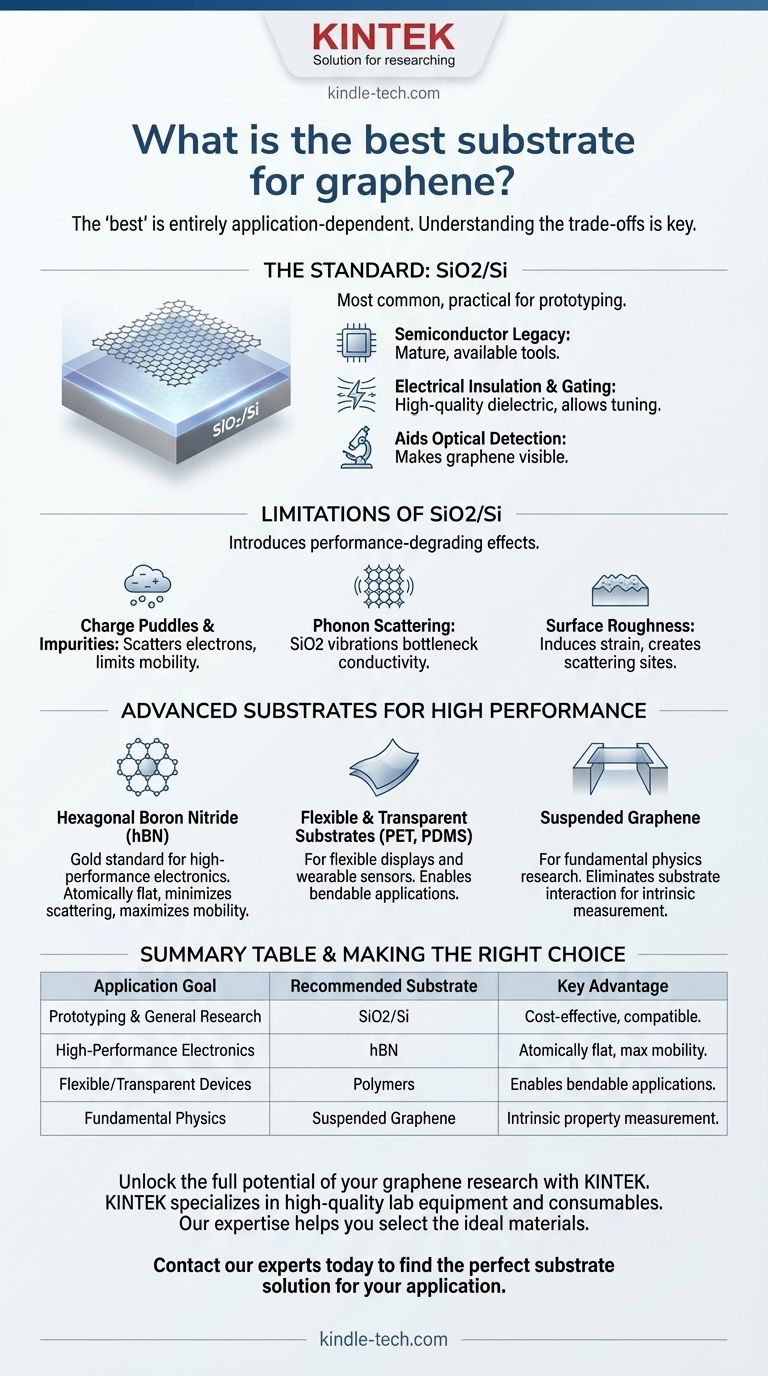
The most common substrate for graphene is silicon dioxide on a silicon wafer (SiO2/Si), but the "best" substrate is entirely dependent on the intended application. SiO2/Si became the standard due to its smooth surface, compatibility with existing semiconductor fabrication technology, and its properties as an electrical insulator, making it a highly practical choice for general research and prototyping.
Choosing the right substrate is not about finding a single 'best' material. It is about understanding the critical trade-offs between electronic performance, optical transparency, mechanical properties, and fabrication scalability for your specific goal.
Why SiO2/Si Became the Standard
The widespread use of SiO2/Si is a direct result of its practical advantages, which were crucial for the initial explosion of graphene research.
The Semiconductor Legacy
Silicon wafers with a thermally grown oxide layer are the bedrock of the entire microelectronics industry.
This means the tools, processes, and knowledge for handling, cleaning, and patterning these substrates are mature and widely available, dramatically lowering the barrier to entry for fabricating graphene devices.
Electrical Insulation and Gating
For electronic applications like transistors, the graphene must be electrically isolated from the conductive silicon wafer. The SiO2 layer serves as a high-quality dielectric insulator.
Furthermore, the highly-doped silicon wafer itself can be used as a "back gate" to apply an electric field, allowing researchers to tune the charge carrier density in the graphene and study its electronic properties.
Aiding Optical Detection
A crucial early breakthrough was the discovery that a specific thickness of SiO2 (typically 285-300 nm) creates a thin-film interference effect.
This effect makes atomically thin, single-layer graphene visible under a standard optical microscope, a simple but vital property that accelerated research significantly.
Understanding the Trade-offs: The Limitations of SiO2/Si
While practical, SiO2/Si is far from perfect. For high-performance applications, it introduces several performance-degrading effects that mask graphene's true potential.
Charge Puddles and Impurities
The surface of SiO2 is not electronically neutral. It contains trapped charges and impurities that create random electrostatic potential variations, often called "charge puddles."
These puddles scatter electrons moving through the graphene, severely limiting its charge carrier mobility and overall electronic performance.
Phonon Scattering
The atoms in the polar SiO2 crystal lattice vibrate in specific ways (known as surface optical phonons).
These vibrations can couple with and scatter the electrons in the graphene, acting as another major bottleneck for its electrical conductivity, especially at room temperature.
Surface Roughness
On an atomic scale, amorphous SiO2 is not perfectly flat. This nanoscale roughness can induce strain and ripples in the overlying graphene sheet, which can alter its electronic structure and create further scattering sites.
Advanced Substrates for High Performance
To overcome the limitations of SiO2/Si, researchers have turned to alternative substrates that better preserve graphene's extraordinary intrinsic properties.
Hexagonal Boron Nitride (hBN)
Often called "white graphene," hBN is considered the gold standard substrate for high-performance graphene electronics.
hBN is an insulating crystal that is atomically flat, free of dangling bonds and surface charge traps, and has a lattice structure very similar to graphene. Encapsulating graphene between layers of hBN minimizes all forms of scattering, allowing for the observation of mobility values near graphene's theoretical limit.
Flexible and Transparent Substrates
For applications in flexible displays, wearable sensors, or transparent conductive films, rigid silicon is unsuitable.
In these cases, polymers like polyethylene terephthalate (PET) or polydimethylsiloxane (PDMS) are used. The primary challenge here is transferring large, high-quality graphene sheets without introducing defects or wrinkles.
Suspended Graphene
For fundamental physics research, the ultimate substrate is no substrate at all.
Suspending a graphene sheet across a trench or hole completely removes any substrate interaction. This allows for the measurement of its true intrinsic properties but is a delicate and complex setup unsuitable for building practical, scalable devices.
Making the Right Choice for Your Goal
Selecting a substrate requires a clear understanding of your primary objective.
- If your primary focus is standard device prototyping or foundational academic research: SiO2/Si remains the most practical and cost-effective choice due to established fabrication processes.
- If your primary focus is maximizing electronic performance and mobility: Hexagonal boron nitride (hBN) is the superior choice, providing an atomically smooth and inert surface.
- If your primary focus is creating flexible electronics or transparent conductors: Polymer substrates like PET or PDMS are necessary to achieve the required mechanical properties.
Ultimately, the best substrate is the one that enables your specific application without compromising its most critical performance metric.
Summary Table:
| Application Goal | Recommended Substrate | Key Advantage |
|---|---|---|
| Prototyping & General Research | SiO2/Si | Cost-effective, widely available, compatible with semiconductor tools |
| High-Performance Electronics | Hexagonal Boron Nitride (hBN) | Atomically flat, minimizes scattering, maximizes mobility |
| Flexible/Transparent Devices | Polymers (PET, PDMS) | Enables bendable, wearable applications |
| Fundamental Physics Research | Suspended Graphene | Eliminates substrate interaction for intrinsic property measurement |
Unlock the full potential of your graphene research with KINTEK.
Choosing the right substrate is critical for your lab's success. Whether you're developing next-generation electronics, flexible sensors, or conducting fundamental research, the substrate you use directly impacts your results.
KINTEK specializes in providing high-quality lab equipment and consumables, including the substrates essential for advanced materials science. Our expertise can help you select the ideal materials to enhance your graphene's performance, streamline your fabrication process, and accelerate your time to discovery.
Let's discuss your project requirements. Contact our experts today to find the perfect substrate solution for your specific application.
Visual Guide
Related Products
- MgF2 Magnesium Fluoride Crystal Substrate Window for Optical Applications
- Optical Window Glass Substrate Wafer Quartz Plate JGS1 JGS2 JGS3
- Optical Window Glass Substrate Wafer Single Double Sided Coated K9 Quartz Sheet
- Conductive Carbon Cloth Carbon Paper Carbon Felt for Electrodes and Batteries
People Also Ask
- How do high-precision temperature controllers and thermocouples influence the conversion efficiency of Magnéli phase?
- Why do we need optical coating? To Control Light and Enhance Optical Performance
- What is the optical coating? Master Light Control for Superior Optical Performance
- What is the effect of substrate on thin films? A Critical Factor for Performance and Reliability
- What do optical coatings do? Control Light for Superior Optical Performance