In the context of MEMS, Chemical Vapor Deposition (CVD) is a fundamental fabrication process used to build thin, solid films of material on top of a substrate, typically a silicon wafer. It works by introducing reactive precursor gases into a chamber, which then undergo a chemical reaction on the heated substrate surface to form the desired material layer, leaving behind gaseous by-products that are exhausted.
At its core, CVD is not merely a coating technique; it is a precise, bottom-up construction method. It allows engineers to build the functional and structural layers of microscopic devices, one atomic layer at a time, directly from a gas phase.

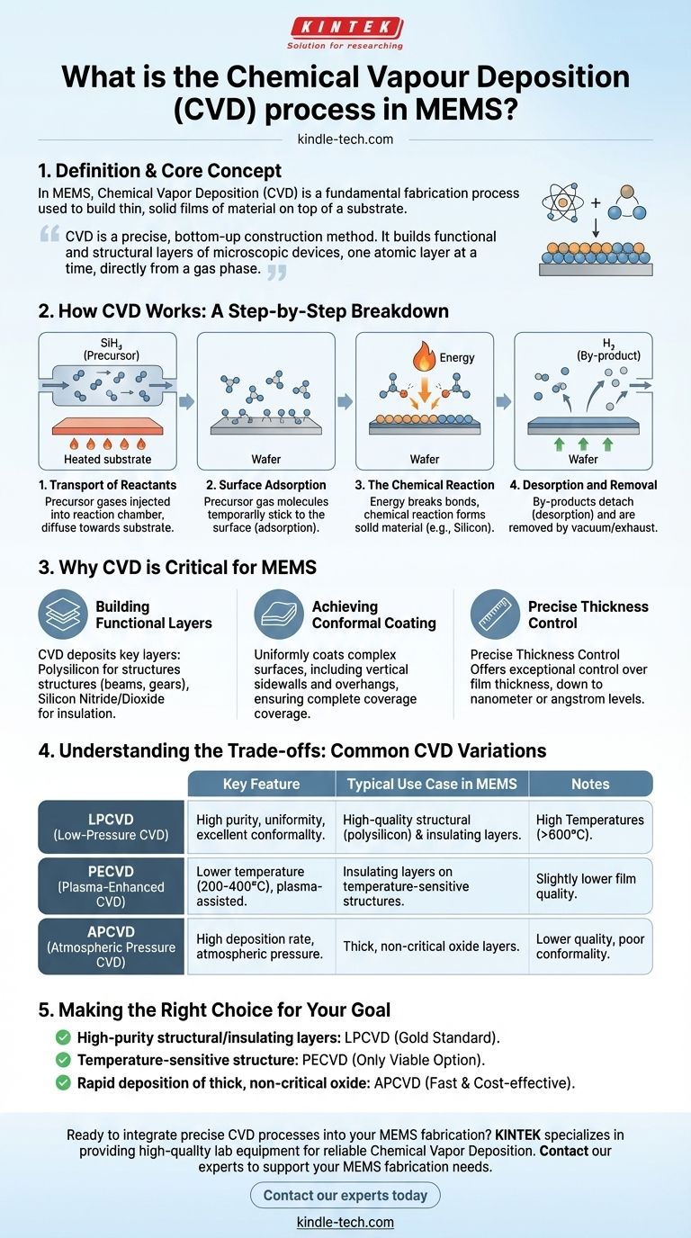
How CVD Works: A Step-by-Step Breakdown
The CVD process can be understood as a sequence of four critical events that transform gas into a solid, high-purity film.
Step 1: Transport of Reactants
Precursor gases, which contain the atoms needed for the final film (e.g., silane, SiH₄, for silicon), are precisely injected into a reaction chamber. These gases diffuse through the chamber and move towards the substrate wafer.
Step 2: Surface Adsorption
Once the precursor gas molecules reach the wafer, they "land" and temporarily stick to the surface. This process, known as adsorption, is a prerequisite for any chemical reaction to occur.
Step 3: The Chemical Reaction
Energy, typically in the form of high temperature, is applied to the substrate. This energy breaks the chemical bonds in the precursor gas molecules, causing a reaction that deposits the desired solid material (like silicon or silicon nitride) onto the surface.
Step 4: Desorption and Removal
The chemical reaction also creates unwanted gaseous by-products (e.g., hydrogen gas from silane). These by-products detach from the substrate surface in a process called desorption and are continuously removed from the chamber by a vacuum or exhaust system.
Why CVD is Critical for MEMS
CVD is not just one of many options; its unique capabilities are essential for creating the complex, three-dimensional structures found in MEMS devices.
Building Functional Layers
MEMS devices are built layer by layer. CVD is the primary method for depositing the most important of these layers, including polysilicon for structural components (like beams and gears) and silicon nitride or silicon dioxide for electrical insulation.
Achieving Conformal Coating
One of the most powerful features of CVD is its ability to produce conformal films. This means the deposited layer uniformly coats all surfaces of a microscopic structure, including vertical sidewalls and underneath overhangs, ensuring complete and reliable coverage.
Precise Thickness Control
The performance of a MEMS device often depends on the precise thickness of its layers. CVD offers exceptional control, allowing for the deposition of films with thicknesses controlled down to the nanometer or even angstrom level.
Understanding the Trade-offs: Common CVD Variations
Different MEMS fabrication steps have different requirements for temperature, film quality, and deposition speed. Consequently, several variations of CVD are used, each with distinct trade-offs.
LPCVD (Low-Pressure CVD)
Operating at very low pressures, LPCVD is the workhorse for high-quality films in MEMS. It produces films with excellent purity, thickness uniformity, and outstanding conformality. Its main trade-off is the requirement for very high temperatures (often >600°C), making it unsuitable for later-stage processing after metals have been deposited.
PECVD (Plasma-Enhanced CVD)
PECVD uses an energy-rich plasma to assist the chemical reaction. This crucial difference allows deposition to occur at much lower temperatures (typically 200-400°C). This makes it essential for depositing insulating layers on top of structures that already contain temperature-sensitive materials like aluminum. The trade-off is often slightly lower film quality and purity compared to LPCVD.
APCVD (Atmospheric Pressure CVD)
As the name implies, this process runs at normal atmospheric pressure. It is very fast and has a high deposition rate, but typically produces lower-quality films with poor conformality. It is mainly used for depositing thick, simple oxide layers where precision is not the primary concern.
Making the Right Choice for Your Goal
Selecting the right CVD process is a critical decision based on the specific requirements of the fabrication step.
- If your primary focus is high-purity structural or insulating layers: LPCVD is the gold standard for creating the core components of a MEMS device.
- If your primary focus is depositing a film on a temperature-sensitive structure: PECVD is the only viable option, protecting previously deposited layers from heat damage.
- If your primary focus is rapid deposition of a thick, non-critical oxide: APCVD offers a fast and cost-effective solution.
Ultimately, Chemical Vapor Deposition is the foundational technique that enables the very construction of the complex, multi-layered architecture of modern micro-devices.
Summary Table:
| CVD Variation | Key Feature | Typical Use Case in MEMS |
|---|---|---|
| LPCVD | High purity & uniformity, excellent conformality | High-quality structural (polysilicon) & insulating layers |
| PECVD | Lower temperature (200-400°C), plasma-assisted | Insulating layers on temperature-sensitive structures |
| APCVD | High deposition rate, atmospheric pressure | Thick, non-critical oxide layers |
Ready to integrate precise CVD processes into your MEMS fabrication? KINTEK specializes in providing the high-quality lab equipment and consumables essential for reliable Chemical Vapor Deposition. Whether you are developing new micro-devices or optimizing your production line, our expertise ensures you achieve the film quality, conformality, and thickness control your projects demand. Contact our experts today to discuss how we can support your laboratory's specific MEMS fabrication needs.
Visual Guide
Related Products
- Microwave Plasma Chemical Vapor Deposition MPCVD Machine System Reactor for Lab and Diamond Growth
- 915MHz MPCVD Diamond Machine Microwave Plasma Chemical Vapor Deposition System Reactor
- Chemical Vapor Deposition CVD Equipment System Chamber Slide PECVD Tube Furnace with Liquid Gasifier PECVD Machine
- Multi Heating Zones CVD Tube Furnace Machine Chemical Vapor Deposition Chamber System Equipment
- Customer Made Versatile CVD Tube Furnace Chemical Vapor Deposition Chamber System Equipment
People Also Ask
- What pressure is needed for chemical vapor deposition of diamonds? Master the Low-Pressure 'Sweet Spot'
- How are CVD diamonds created? Discover the Science of Lab-Grown Diamond Precision
- What are the primary advantages of the CVD method for growing diamonds? Engineering High-Purity Gems and Components
- How does MPCVD work? A Guide to Low-Temperature, High-Quality Film Deposition
- What is microwave plasma chemical vapor deposition? A Guide to High-Purity Diamond Film Growth


