At its core, DC (Direct Current) sputtering is a vacuum deposition technique used to create ultra-thin films of material. The process works by creating a plasma from an inert gas, which generates high-energy ions. These ions are accelerated by a DC voltage to bombard a source material (the "target"), physically knocking atoms off its surface, which then travel and deposit onto a substrate, forming a uniform coating.
The central principle of DC sputtering is not a chemical reaction but a physical one based on momentum transfer. Think of it as a microscopic game of billiards, where an energized gas ion is the cue ball, striking atoms in the target material and knocking them out so they can land precisely on a nearby substrate.
The Core Mechanism: From Plasma to Film
To understand DC sputtering, it helps to break it down into a sequence of events that occur within the vacuum chamber.
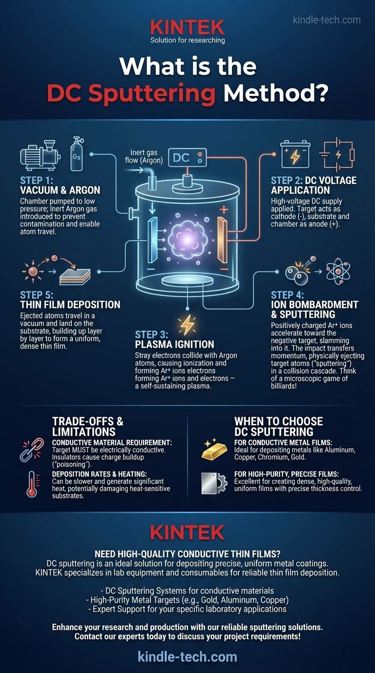
Step 1: Creating the Vacuum Environment
The entire process happens in a vacuum chamber pumped down to a very low pressure. An inert gas, most commonly Argon (Ar), is then introduced.
This vacuum is critical for two reasons: it prevents the target material and substrate from being contaminated by atmospheric particles, and it ensures the sputtered atoms can travel from the target to the substrate without colliding with other gas molecules.
Step 2: Applying the DC Voltage
A high-voltage DC power supply is connected to the components inside the chamber. The source material, or target, is set up as the cathode (negative charge).
The substrate holder and the chamber walls typically act as the anode (positive charge). This creates a strong electric field between the target and the anode.
Step 3: Igniting the Plasma
This electric field accelerates stray free electrons present in the chamber. As these high-speed electrons collide with the neutral Argon gas atoms, they knock electrons out of the Argon atoms' shells.
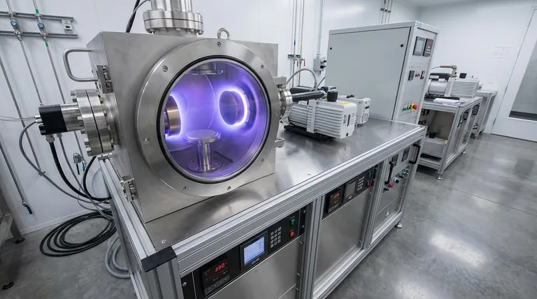
This process, called ionization, creates positively charged Argon ions (Ar+) and more free electrons. This self-sustaining cloud of ions and electrons is the plasma, which often has a characteristic glow.
Step 4: The Bombardment Process
The positively charged Argon ions (Ar+) are now strongly attracted to the negatively charged target. They accelerate across the electric field and slam into the target's surface with significant kinetic energy.
This impact initiates a "collision cascade" within the target material, transferring momentum from the ion to the target's atoms. When this cascade of energy reaches the surface, it can be enough to overcome the material's atomic binding energy, causing a target atom to be physically ejected or "sputtered."
Step 5: Deposition on the Substrate
The ejected atoms from the target travel in a straight line through the vacuum until they strike a surface. By strategically placing a substrate (such as a silicon wafer, glass, or plastic part) in front of the target, these atoms land on it.
Over time, these atoms build up, layer by layer, to form a thin, dense, and highly uniform film on the substrate's surface.
Understanding the Trade-offs and Limitations
While powerful, DC sputtering is not a universal solution. Understanding its inherent limitations is key to using it effectively.
The Conductive Material Requirement
The primary limitation of DC sputtering is that the target material must be electrically conductive. The process relies on a constant negative charge on the target to attract the positive ions.
If the target is an insulator (a dielectric material), the bombardment of positive ions will cause a charge buildup on the surface. This positive charge neutralizes the negative potential of the cathode, effectively repelling further ions and shutting the sputtering process down. This is often called "target poisoning."
Deposition Rates and Heating
Compared to some other methods like thermal evaporation, basic DC sputtering can have a relatively low deposition rate, making it a slower process.
Furthermore, the constant bombardment of energetic particles can transfer significant heat to the substrate, which may damage heat-sensitive materials like certain plastics or organic layers.
When to Choose DC Sputtering
Your choice of deposition method depends entirely on your material and desired outcome.
- If your primary focus is depositing a conductive metal film: DC sputtering is a highly reliable, predictable, and well-understood industry standard for materials like aluminum, copper, chromium, and gold.
- If you require high-purity films with precise thickness control: The vacuum environment and controlled physical bombardment of sputtering make it an excellent choice for creating dense, high-quality films.
- If you need to coat a non-conductive (dielectric) material: You must look beyond DC sputtering to methods like RF (Radio Frequency) sputtering, which is specifically designed to overcome the issue of charge buildup on insulating targets.
Understanding this fundamental process is the first step toward controlling the properties of materials at the atomic scale.
Summary Table:
| Aspect | Description |
|---|---|
| Process Type | Physical Vapor Deposition (PVD) |
| Key Requirement | Target material must be electrically conductive |
| Common Applications | Deposition of metals (e.g., Al, Cu, Au, Cr) |
| Primary Advantage | Creates dense, high-purity, uniform thin films |
| Main Limitation | Cannot be used with insulating (dielectric) target materials |
Need High-Quality Conductive Thin Films?
DC sputtering is an ideal solution for depositing precise, uniform metal coatings. KINTEK specializes in providing the lab equipment and consumables you need to achieve reliable thin film deposition.
We supply:
- DC Sputtering Systems for conductive materials
- High-Purity Metal Targets (e.g., Gold, Aluminum, Copper)
- Expert Support for your specific laboratory applications
Enhance your research and production with our reliable sputtering solutions. Contact our experts today to discuss your project requirements!
Visual Guide
Related Products
- Spark Plasma Sintering Furnace SPS Furnace
- Vacuum Induction Melting Spinning System Arc Melting Furnace
- Circulating Water Vacuum Pump for Laboratory and Industrial Use
People Also Ask
- What is the mechanism of SPS process? A Deep Dive into Rapid, Low-Temperature Sintering
- What is the theory of spark plasma sintering? A Guide to Rapid, Low-Temperature Densification
- Why are Spark Plasma Sintering (SPS) furnaces or hot presses utilized in the preparation of Li3PS4 solid electrolytes?
- What are the fundamentals of spark plasma sintering process? Unlock Rapid, High-Performance Material Consolidation
- What is the difference between spark plasma sintering and flash sintering? A Guide to Advanced Sintering Methods


