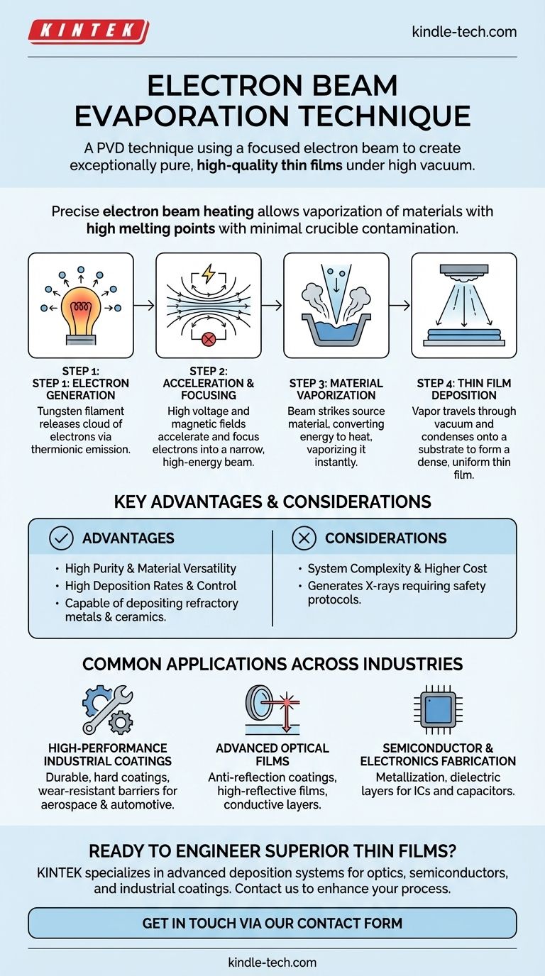
At its core, electron beam evaporation is a physical vapor deposition (PVD) technique used to create exceptionally pure, high-quality thin films. It operates within a high vacuum by directing a focused beam of high-energy electrons at a source material, converting the electrons' kinetic energy into intense thermal energy. This heat vaporizes the material, which then travels and condenses onto a substrate to form the desired coating.
The central principle of electron beam evaporation is its ability to use a precisely controlled electron beam for highly localized heating. This allows for the vaporization of a vast range of materials, including those with very high melting points, while minimizing contamination from the crucible holding the material.
How It Works: A Step-by-Step Breakdown
To understand this technique, it's best to visualize the process from electron emission to film formation. Each step is carefully controlled to achieve the desired film properties.
Step 1: Electron Generation
The process begins at a tungsten filament inside an "electron gun." A high electric current is passed through this filament, causing it to heat up significantly through a process known as Joule heating.
This intense heat provides enough energy for the filament to release a cloud of electrons via thermionic emission.
Step 2: Acceleration and Focusing
Once emitted, these free electrons are accelerated toward the source material by a powerful electric field, typically created by a high voltage between 5 and 10 kV.
Simultaneously, a magnetic field is applied to focus these accelerated electrons into a narrow, high-energy beam. This precision is critical for controlling where the energy is delivered.
Step 3: Material Vaporization
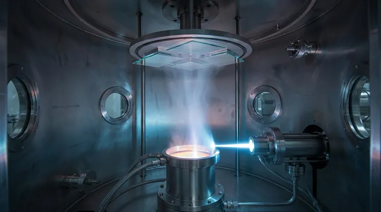
The focused electron beam strikes the surface of the source material, which is held in a water-cooled copper crucible. Upon impact, the immense kinetic energy of the electrons is instantly converted into thermal energy.
This energy transfer creates a small, superheated molten pool on the material's surface, causing it to rapidly evaporate (or sublimate, for some materials) into a gaseous vapor phase.
Step 4: Thin Film Deposition
This vapor then travels in a straight line through the high-vacuum chamber. When the vapor stream reaches the comparatively cool substrate placed above the source, it condenses back into a solid state.
This condensation process builds up, layer by layer, to form a dense and uniform thin film on the substrate's surface.
Understanding the Key Advantages and Trade-offs
Electron beam evaporation is a powerful technique, but its suitability depends on the specific application. Understanding its trade-offs is crucial for making an informed decision.
Advantage: High Purity and Material Versatility
Because the water-cooled crucible remains cool, only the material struck by the electron beam is heated. This prevents the crucible itself from melting or outgassing, which significantly reduces film contamination.
This method can also vaporize materials with extremely high melting points, such as refractory metals and ceramics, which are impossible to deposit with simpler thermal evaporation techniques.
Advantage: High Deposition Rates and Control
The energy density of the electron beam allows for very high and controllable deposition rates. This makes the process efficient for both research and industrial-scale production.
Reactive gases like oxygen or nitrogen can also be introduced into the chamber to form specific compound films, such as dielectric oxides or hard nitrides.
Consideration: System Complexity and Safety
E-beam systems are more complex and expensive than other PVD methods like thermal evaporation. They require high-voltage power supplies, magnetic focusing coils, and sophisticated control systems.
Furthermore, the impact of high-energy electrons on the target material generates X-rays as a byproduct. This requires appropriate shielding and safety protocols to protect both operators and sensitive electronic components.
Common Applications Across Industries
The precision and purity of e-beam evaporation make it indispensable in demanding fields where film quality is paramount.
High-Performance Industrial Coatings
This technique is used to create durable, hard coatings for cutting tools and wear-resistant thermal barrier coatings for aerospace and automotive engine components. It also provides chemical barriers for parts exposed to corrosive environments.
Advanced Optical Films
It is a go-to method for manufacturing complex optical coatings. Applications include anti-reflection coatings for lenses and eyeglasses, highly reflective films for lasers and mirrors, and conductive layers for solar panels and architectural glass.
Semiconductor and Electronics Fabrication
In the electronics industry, e-beam evaporation is used for metallization to create conductive pathways on integrated circuits and for depositing the thin dielectric layers essential for components like capacitors and Josephson junctions.
Making the Right Choice for Your Goal
Selecting the right deposition technique requires aligning its capabilities with your primary objective.
- If your primary focus is creating high-purity optical films or complex dielectric stacks: E-beam evaporation is the superior choice due to its precise rate control and minimal contamination.
- If your primary focus is depositing refractory metals or materials with very high melting points: E-beam is one of the few techniques capable of delivering the necessary energy efficiently.
- If your primary focus is simple, low-cost metallization with common materials like aluminum or gold: A simpler technique like thermal evaporation might be a more cost-effective solution.
Ultimately, electron beam evaporation provides an unparalleled level of control and purity for engineering advanced thin films.
Summary Table:
| Key Feature | Description |
|---|---|
| Process | Physical Vapor Deposition (PVD) using a focused electron beam |
| Primary Advantage | High-purity films; ability to deposit high-melting-point materials |
| Typical Applications | Optical coatings, semiconductor metallization, industrial wear coatings |
| Material Versatility | Metals, ceramics, refractory materials |
Ready to engineer superior thin films for your application?
KINTEK specializes in high-performance lab equipment, including advanced deposition systems. Whether you are developing cutting-edge optics, semiconductor devices, or durable industrial coatings, our expertise and solutions can help you achieve the purity and precision your work demands.
Contact us today to discuss how our equipment can enhance your research and production processes. Get in touch via our contact form to speak with an expert.
Visual Guide
Related Products
- Electron Beam Evaporation Coating Tungsten Crucible and Molybdenum Crucible for High Temperature Applications
- Electron Beam Evaporation Coating Oxygen-Free Copper Crucible and Evaporation Boat
- Electron Beam Evaporation Coating Gold Plating Tungsten Molybdenum Crucible for Evaporation
- Electron Beam Evaporation Coating Conductive Boron Nitride Crucible BN Crucible
- E Beam Crucibles Electron Gun Beam Crucible for Evaporation
People Also Ask
- What is the current of e-beam evaporation? A Guide to High-Purity Thin Film Deposition
- What materials are used in electron beam evaporation? Master High-Purity Thin Film Deposition
- What is the voltage of e-beam evaporation? Achieve Precise Thin-Film Deposition
- What is e-beam evaporation used for? Precision Coating for Optics, Aerospace & Electronics
- What are the applications of e-beam evaporation? Achieve High-Purity Coatings for Optics & Electronics


