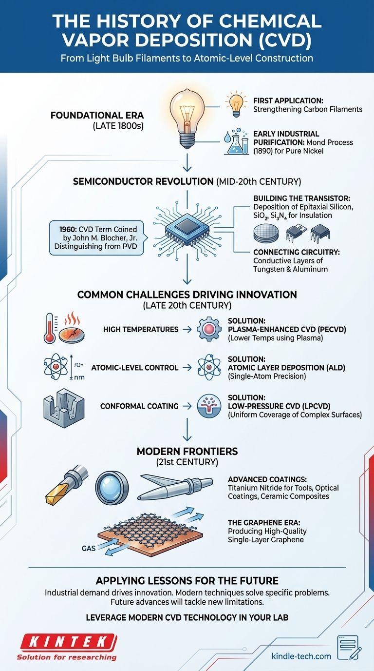
The history of chemical vapor deposition (CVD) reveals a technology whose core principles were observed over a century ago but were only formally defined and rapidly advanced with the dawn of the semiconductor age. While the term was coined by John M. Blocher, Jr. in 1960 to distinguish it from physical methods, its roots trace back to early experiments with incandescent light bulbs in the late 19th century.
The evolution of CVD is a clear story of a scientific principle being transformed by industrial necessity. It grew from a niche technique for simple coatings into the atomic-level construction tool that underpins virtually all modern electronics and advanced materials.
The Foundational Era: Early Discoveries
The fundamental concept of using a chemical reaction in a gaseous state to create a solid deposit has been in practice far longer than the formal name has existed.
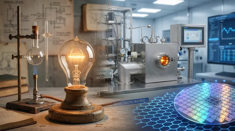
The First Application: Light Bulb Filaments
In the late 1800s, innovators working on the incandescent light bulb faced the challenge of brittle carbon filaments. They discovered that heating these filaments in a hydrocarbon gas atmosphere would decompose the gas, depositing a layer of carbon that significantly increased the filament's strength and lifespan. This was, in essence, the first major industrial use of CVD.
Early Industrial Purification
Around the same time, the Mond process was developed in 1890 to refine nickel. This process involved reacting impure nickel with carbon monoxide to form a volatile gas (nickel carbonyl), which was then decomposed by heat in a separate chamber to deposit ultra-pure nickel. This demonstrated the power of CVD for creating materials of exceptionally high purity.
The Semiconductor Revolution: A New Demand for Precision
The mid-20th century marked the most critical turning point in CVD's history. The rise of the electronics industry created a demand that only CVD could meet.
A Formal Definition
In 1960, John M. Blocher, Jr. officially proposed the term Chemical Vapor Deposition. This act was crucial, as it formally established CVD as a distinct field of materials science, separating it from Physical Vapor Deposition (PVD), which involves processes like evaporation or sputtering.
Building the Transistor
The development of the integrated circuit required the ability to lay down incredibly thin, pure, and uniform layers of different materials. CVD became the go-to method for depositing the epitaxial silicon that forms the foundation of a microchip, as well as the silicon dioxide and silicon nitride films used for insulation.
Connecting the Circuitry
As circuits became more complex, CVD was also adapted to deposit conductive layers. Techniques were developed to deposit metals like tungsten and aluminum, which serve as the microscopic wiring connecting the millions of transistors on a single chip.
Common Challenges That Drove Innovation
The history of CVD is not just one of success, but also of overcoming fundamental limitations. These challenges were the primary catalysts for the development of more advanced CVD techniques.
The Problem of High Temperatures
Traditional CVD processes require very high temperatures to drive the necessary chemical reactions. This heat can damage or alter the delicate, pre-existing layers on a semiconductor wafer. This limitation directly led to the invention of Plasma-Enhanced CVD (PECVD), which uses an energy-rich plasma to allow deposition to occur at much lower, safer temperatures.
The Pursuit of Atomic-Level Control
As electronic components shrank to the nanometer scale, manufacturers needed to control film thickness with single-atom precision. This seemingly impossible demand spurred the development of Atomic Layer Deposition (ALD), a sub-class of CVD where precursor gases are pulsed into the chamber one at a time, allowing for the growth of a material one perfect atomic layer at a time.
The Need for Conformal Coating
Early CVD methods struggled to evenly coat the complex, three-dimensional trenches and structures of a modern microchip. This led to the creation of Low-Pressure CVD (LPCVD), a technique that improves the ability of precursor gases to reach and coat all surfaces uniformly, ensuring no gaps or defects.
Modern Frontiers: Beyond Electronics
While its development was driven by electronics, the applications of CVD have expanded dramatically into nearly every field of engineering and materials science.
Advanced Coatings and Materials
Today, CVD is used to apply ultra-hard titanium nitride coatings to cutting tools, create scratch-resistant optical coatings for lenses, and manufacture high-performance ceramic composites for the aerospace industry.
The Graphene Era
More recently, CVD has become the leading method for producing large, high-quality, single-layer sheets of graphene. By flowing methane gas over a heated copper foil, researchers can grow uniform graphene films, unlocking the material's potential for next-generation electronics, sensors, and composites.
Applying These Historical Lessons
Understanding the evolution of CVD provides a clear framework for appreciating its role in technology today.
- If your primary focus is process selection: Recognize that modern techniques like PECVD and ALD were developed to solve specific problems (heat and precision) inherent in older methods.
- If your primary focus is materials science: Note that industrial demand, particularly from the semiconductor sector, has been the single greatest driver of innovation in thin-film deposition.
- If your primary focus is future development: Understand that the next great advance in deposition technology will likely arise from a fundamental limitation encountered in producing tomorrow's technology.
CVD's journey from strengthening a simple filament to building the most complex devices known to humanity is a testament to its unparalleled versatility and control.
Summary Table:
| Era | Key Development | Impact |
|---|---|---|
| Late 1800s | Strengthening carbon filaments in light bulbs | First industrial use of CVD principles |
| 1890 | Mond process for nickel purification | Demonstrated CVD's ability to create high-purity materials |
| 1960 | Term "CVD" coined by John M. Blocher, Jr. | Formalized the field, distinguishing it from PVD |
| Mid-20th Century | Deposition of epitaxial silicon, SiO₂, Si₃N₄ for semiconductors | Became foundational to the integrated circuit and electronics industry |
| Late 20th Century | Development of PECVD, LPCVD, ALD | Solved challenges of high temperature, conformality, and atomic-level precision |
| 21st Century | Production of graphene and advanced coatings | Expanded into new materials for electronics, aerospace, and optics |
Ready to leverage the precision of modern CVD technology in your lab?
The history of CVD shows how solving material deposition challenges drives innovation. KINTEK specializes in providing the advanced lab equipment and consumables needed for cutting-edge research and production. Whether you are developing next-generation semiconductors, graphene-based devices, or high-performance coatings, we have the solutions to support your work.
Contact us today to discuss how our expertise can enhance your laboratory's capabilities. Let's build the future of materials science together. Get in touch via our contact form
Visual Guide
Related Products
- Chemical Vapor Deposition CVD Equipment System Chamber Slide PECVD Tube Furnace with Liquid Gasifier PECVD Machine
- RF PECVD System Radio Frequency Plasma-Enhanced Chemical Vapor Deposition RF PECVD
- Microwave Plasma Chemical Vapor Deposition MPCVD Machine System Reactor for Lab and Diamond Growth
- Customer Made Versatile CVD Tube Furnace Chemical Vapor Deposition Chamber System Equipment
- 915MHz MPCVD Diamond Machine Microwave Plasma Chemical Vapor Deposition System Reactor
People Also Ask
- What are the processes of vapor phase deposition? Understand CVD vs. PVD for Superior Thin Films
- What types of substrates are used in CVD to facilitate graphene films? Optimize Graphene Growth with the Right Catalyst
- What is plasma enhanced chemical vapor deposition PECVD equipment? A Guide to Low-Temperature Thin Film Deposition
- How are carbon nanotubes grown? Master Scalable Production with Chemical Vapor Deposition
- What are the core advantages of PE-CVD in OLED encapsulation? Protect Sensitive Layers with Low-Temp Film Deposition


