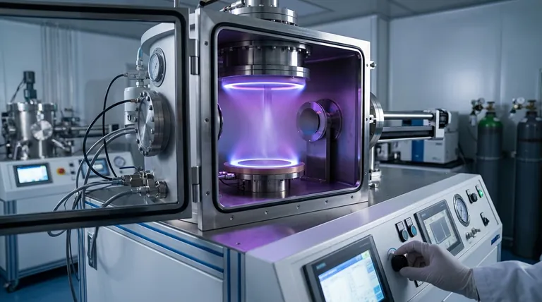
At its core, magnetron sputtering is a highly controlled vacuum deposition technique used to create ultra-thin films of material. It works by creating a plasma, using it to bombard a source material (the "target"), and physically knocking atoms off the target so they can deposit onto a substrate. The key innovation is the use of a magnetic field to intensify the plasma, dramatically increasing the efficiency and speed of the coating process.
The central purpose of magnetron sputtering is not just to deposit a thin film, but to do so with exceptional control and speed. It leverages a magnetic field to create a dense, localized plasma, enabling higher deposition rates and lower process temperatures than standard sputtering methods.
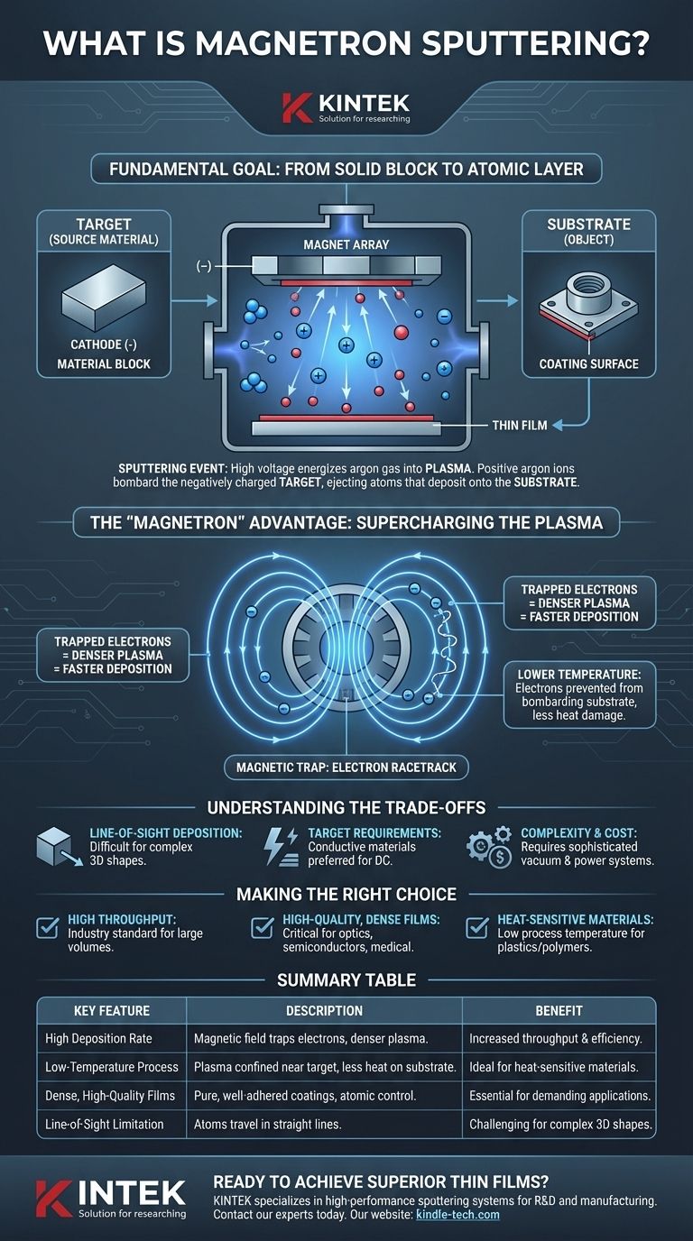
The Fundamental Goal: From Solid Block to Atomic Layer
Magnetron sputtering is a refined form of a process called Physical Vapor Deposition (PVD). The objective of any PVD technique is to take a solid material, convert it into a vapor state, and then have it condense onto a surface as a solid, high-performance coating.
The Target: The Source Material
The process begins with the target, which is a block of the material you wish to deposit. This target acts as a cathode, meaning it is given a strong negative electrical charge.
The Substrate: The Object to Be Coated
The substrate is the component or part that will receive the coating. It is placed within the vacuum chamber, positioned to face the target.
The Sputtering Event: An Atomic Collision
To start the process, a high voltage is applied across a low-pressure gas (typically argon) inside a vacuum chamber. This energizes the gas, stripping electrons from the argon atoms and creating plasma—an ionized gas of positive argon ions and free electrons.
Attracted by the negatively charged target, these positive argon ions accelerate and collide with the target's surface with great force. This impact has enough energy to physically knock out, or "sputter," individual atoms from the target material. These ejected atoms then travel through the vacuum and deposit onto the substrate, building up a thin film one atom at a time.
The "Magnetron" Advantage: Supercharging the Plasma
Simple sputtering works, but it can be slow and inefficient. The addition of a magnetic field—the "magnetron" part—revolutionizes the process by enhancing the plasma exactly where it is needed most.
The Magnetic Trap
A powerful magnetic field is applied from behind the target. This field is invisible but has a profound effect on the charged particles in the plasma, particularly the lightweight electrons.
Instead of escaping into the chamber, the electrons become trapped by the magnetic field, forcing them into a long, spiral path very close to the target's surface. Think of it as creating a high-speed racetrack for electrons directly in front of the target.
The Cascade Effect: Denser Plasma, Faster Deposition
These trapped, rapidly moving electrons have a much higher probability of colliding with neutral argon atoms. Each collision creates another positive argon ion, which is then accelerated into the target to sputter more material.
This cascade effect creates a significantly denser and more intense plasma confined near the target. A denser plasma means more ion bombardment, which directly translates to a much higher deposition rate.
Lower Temperature, Less Damage
A critical benefit of trapping the electrons near the target is that they are prevented from bombarding the substrate. This significantly reduces the amount of heat transferred to the part being coated, allowing for the successful coating of heat-sensitive materials like plastics and polymers.
Understanding the Trade-offs
While powerful, magnetron sputtering is not a universal solution. Understanding its limitations is key to using it effectively.
Line-of-Sight Deposition
The sputtered atoms travel in a relatively straight line from the target to the substrate. This means it is difficult to uniformly coat complex, three-dimensional shapes with deep recesses or hidden surfaces without sophisticated substrate manipulation.
Target Material Requirements
Standard DC magnetron sputtering works best with electrically conductive target materials, as the target must be able to hold a negative charge. Coating insulating or dielectric materials (like ceramics) requires a more complex setup, such as Radio Frequency (RF) or pulsed-DC sputtering, to prevent charge buildup.
System Complexity and Cost
Magnetron sputtering systems are sophisticated pieces of equipment. They require high-vacuum chambers, precise gas flow controllers, high-voltage power supplies, and powerful magnet arrays, making the initial investment and maintenance significant.
Making the Right Choice for Your Goal
Selecting a coating process depends entirely on your technical and commercial objectives. Here is how to decide if magnetron sputtering aligns with your needs.
- If your primary focus is high throughput and industrial scale: Magnetron sputtering is an industry standard for its high deposition rates, making it ideal for efficiently coating large volumes of components.
- If your primary focus is a high-quality, dense film: The process produces exceptionally dense, pure, and well-adhered coatings, which is critical for demanding applications in optics, semiconductors, and medical devices.
- If your primary focus is coating heat-sensitive materials: The relatively low process temperature makes it one of the best choices for applying high-performance coatings onto plastics, polymers, or other substrates that cannot withstand high heat.
By mastering the physics of plasma and magnetic fields, magnetron sputtering offers precise control over the properties of materials at the atomic level.
Summary Table:
| Key Feature | Description | Benefit |
|---|---|---|
| High Deposition Rate | Magnetic field traps electrons, creating a dense plasma for faster atom ejection. | Increased throughput and efficiency for industrial applications. |
| Low-Temperature Process | Plasma is confined near the target, minimizing heat damage to the substrate. | Ideal for coating heat-sensitive materials like plastics and polymers. |
| Dense, High-Quality Films | Produces pure, well-adhered coatings with precise atomic-level control. | Essential for demanding applications in optics, semiconductors, and medical devices. |
| Line-of-Sight Limitation | Sputtered atoms travel in straight lines from the target. | Can be challenging for uniform coating of complex 3D shapes without part manipulation. |
Ready to achieve superior thin films for your laboratory or production line?
KINTEK specializes in high-performance lab equipment, including sputtering systems designed for precision, reliability, and efficiency. Whether you are in R&D or manufacturing, our solutions help you deposit high-quality coatings on everything from semiconductors to medical devices.
Contact our experts today to discuss how our sputtering technology can meet your specific material deposition goals.
Visual Guide
Related Products
- Three-dimensional electromagnetic sieving instrument
- Chemical Vapor Deposition CVD Equipment System Chamber Slide PECVD Tube Furnace with Liquid Gasifier PECVD Machine
People Also Ask
- Why is sieving equipment essential for the classification of processed bio-activated carbon? Optimize Performance
- What are advantages and disadvantages of sieving method? A Guide to Reliable & Cost-Effective Particle Sizing
- What are the precautions for sieving method? Ensure Accurate Particle Size Analysis
- What mixtures can be separated by sieving? A Guide to Efficient Solid-Solid Separation
- What type of materials can be separated using the method of sieving? A Guide to Efficient Particle Size Separation

