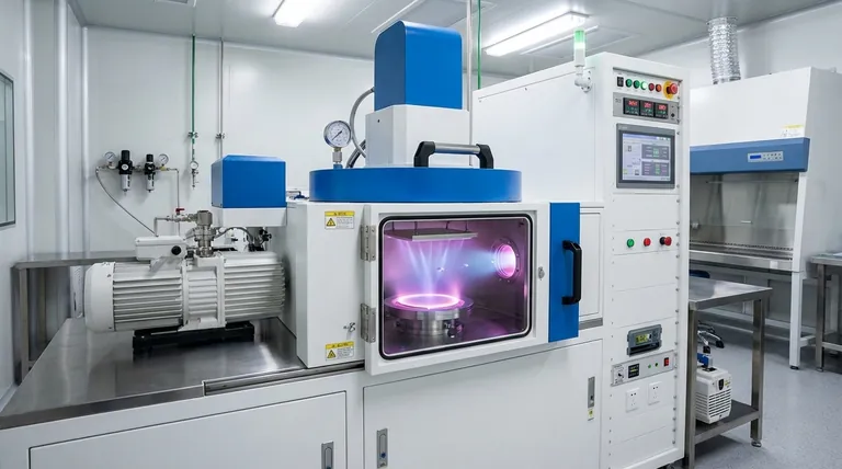
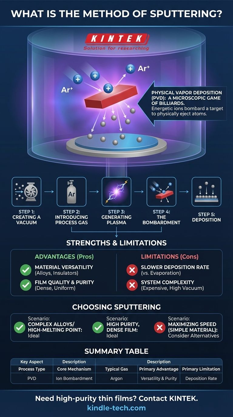
In essence, sputtering is a physical vapor deposition (PVD) method used to create ultra-thin films. The process occurs in a vacuum and involves using energetic ions from a gas plasma to bombard a source material, known as a target. This collision physically ejects or "sputters" atoms from the target, which then travel and deposit onto a substrate, forming a uniform coating.
Sputtering is fundamentally a physical process, not a chemical one. Think of it as a microscopic game of billiards where energetic gas ions are used to knock atoms off a source material, which then deposit onto a surface to form an ultra-thin, high-purity film.
The Core Mechanism of Sputtering
To truly understand sputtering, it is best to break it down into a sequence of distinct steps. Each step is critical for controlling the final properties of the deposited film.
Step 1: Creating a Vacuum
The entire process must take place in a vacuum chamber. This is done to remove atmospheric gases and contaminants like oxygen, nitrogen, and water vapor, which could otherwise react with the sputtered material and compromise the purity of the thin film.
Step 2: Introducing a Process Gas
Once a high vacuum is achieved, the chamber is backfilled with a small, controlled amount of an inert process gas, which is almost always argon. Argon is used because it is chemically non-reactive and has a suitable atomic mass to effectively eject atoms from the target.
Step 3: Generating a Plasma
An electrical potential is applied within the chamber, which energizes the argon gas and ignites a plasma. This plasma is a glowing, ionized state of gas containing a mix of positive argon ions (Ar+) and free electrons.
Step 4: The Bombardment
The source material, or target, is given a negative electrical charge. This causes the positively charged argon ions from the plasma to accelerate aggressively toward the target, striking its surface with significant kinetic energy.
Step 5: Deposition on the Substrate
This energetic bombardment physically knocks atoms loose from the target's surface. These ejected atoms travel through the low-pressure chamber until they strike a surface, which is the object to be coated, known as the substrate. They then condense on the substrate, gradually building up a thin, uniform film.
Understanding the Strengths and Limitations
Like any technical process, sputtering has distinct advantages and trade-offs. Recognizing these is key to deciding if it's the right method for a specific application.
Key Advantage: Material Versatility
Because sputtering is a physical momentum-transfer process, it is not limited by material properties like melting point. It can deposit high-melting-point metals, complex alloys with their composition intact, and even electrically insulating materials, making it exceptionally versatile.
Key Advantage: Film Quality and Purity
The high-vacuum environment ensures that the resulting films are extremely pure and dense. The process offers precise control over film thickness and uniformity across the substrate surface.
Limitation: Deposition Rate
Generally, sputtering has a slower deposition rate compared to other methods like thermal evaporation. This can make it less economical for applications requiring very thick coatings or high-volume throughput.
Limitation: System Complexity
Sputtering systems are relatively complex and expensive. They require high-vacuum pumps, sophisticated power supplies to generate the plasma, and precise gas flow controllers, which can represent a significant capital investment.
Choosing Sputtering for Your Application
Your final decision should be guided by the specific requirements of your end product. The unique characteristics of sputtering make it ideal for certain goals but less suitable for others.
- If your primary focus is coating with complex alloys or high-melting-point metals: Sputtering offers superior control over composition and stoichiometry that other methods struggle to achieve.
- If your primary focus is creating a high-purity, dense film on virtually any substrate: The clean, controlled vacuum environment and physical nature of sputtering make it the ideal choice for high-performance applications.
- If your primary focus is maximizing deposition speed for a simple, low-melting-point material: You may want to evaluate other PVD methods like thermal evaporation, which can offer faster throughput.
By understanding its core physical nature, you can leverage sputtering to create high-performance coatings that are simply not possible with many other techniques.
Summary Table:
| Key Aspect | Description |
|---|---|
| Process Type | Physical Vapor Deposition (PVD) |
| Core Mechanism | Energetic ion bombardment ejects target atoms |
| Typical Gas | Argon (inert) |
| Primary Advantage | Deposits high-melting-point metals, alloys, and insulators |
| Primary Limitation | Slower deposition rate than some alternatives |
Need a high-purity, uniform thin film for your lab? KINTEK specializes in sputtering equipment and consumables, delivering precise control for coating complex alloys and high-performance substrates. Our solutions ensure exceptional film quality and purity for your most demanding applications. Contact our experts today to discuss how we can enhance your laboratory's capabilities!
Visual Guide
Related Products
- Lab Sterile Slapping Type Homogenizer for Tissue Mashing and Dispersing
- Spark Plasma Sintering Furnace SPS Furnace
- Single Punch Manual Tablet Press Machine TDP Tablet Punching Machine
People Also Ask
- What role does a laboratory homogenizer play in radioactive cesium detection? Ensure Accuracy in Wildlife Sampling
- Why is maintaining nanoparticle dispersion critical for photocatalytic reactors? Maximize Your Reaction Efficiency
- What is the role of an ultrasonic cleaner during magnesium alloy coating? Ensure Superior Adhesion and Surface Purity
- What role does an ultrasonic cleaner play in the pre-treatment of 4140 steel? Ensure Uniform Nitriding Activation
- How does a laboratory automatic masticator or homogenizer facilitate the processing of biofilm samples? Optimize Accuracy


