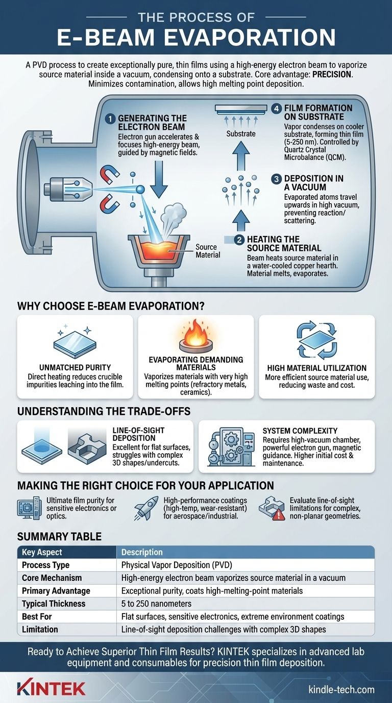
At its core, e-beam evaporation is a physical vapor deposition (PVD) process used to create exceptionally pure, thin films. The technique uses a high-energy beam of electrons to heat a source material inside a vacuum chamber until it vaporizes. This vapor then travels and condenses onto a target object, or substrate, forming a uniform coating.
The fundamental advantage of e-beam evaporation is its precision. By directly heating only the source material with electrons, the process minimizes contamination and allows for the deposition of materials with very high melting points, resulting in superior film quality.
The Core Mechanism: From Electron to Film
The entire process occurs within a high-vacuum environment, which is critical for ensuring the purity of the film and allowing vaporized atoms to travel freely to the substrate.
Generating the Electron Beam
The process begins with an electron gun that accelerates a stream of electrons into a focused, high-energy beam. This beam is precisely guided by magnetic fields.
Heating the Source Material
The electron beam is directed onto the source material—the substance intended for the film—which rests in a water-cooled copper hearth or crucible. The intense energy from the electrons rapidly heats the material, causing it to melt and then evaporate, transitioning into a gaseous state.
The water-cooled hearth is a key design element, as it prevents the crucible itself from melting and contaminating the process.
Deposition in a Vacuum
The evaporated atoms or molecules travel upwards in a straight line through the vacuum chamber. The absence of air or other gases prevents the vapor from reacting or scattering before it reaches its destination.
Film Formation on the Substrate
A substrate is positioned directly above the evaporating source. As the vaporized particles strike the cooler surface of the substrate, they condense back into a solid state, gradually building up a thin film layer by layer.
Controlling Thickness and Purity
To ensure precision, systems use tools like a Quartz Crystal Microbalance (QCM). This device monitors the rate of deposition in real-time, allowing for exact control over the final film thickness, which typically ranges from 5 to 250 nanometers.
Why Choose E-Beam Evaporation?
E-beam evaporation is not just one of many options; it is often the best choice for applications demanding the highest quality and performance.
Achieving Unmatched Purity
Because the electron beam heats the source material directly and locally, there is very little heat transfer to the crucible. This significantly reduces the risk of impurities from the container leaching into the film, resulting in a coating of exceptionally high purity.
Evaporating Demanding Materials
The focused, high-energy nature of the electron beam makes it possible to evaporate materials with very high melting points, such as refractory metals and ceramics. Other heating methods often cannot generate sufficient temperatures to vaporize these materials effectively.
High Material Utilization
Compared to other PVD techniques, e-beam evaporation can be more efficient in its use of source material. This efficiency reduces waste and can lower the overall cost, especially when working with expensive materials.
Understanding the Trade-offs
While powerful, the process has inherent characteristics that make it ideal for some applications but less suitable for others. Understanding these trade-offs is key to making an informed decision.
Line-of-Sight Deposition
The evaporated material travels in a straight line from the source to the substrate. This "line-of-sight" characteristic means it is excellent for coating flat surfaces but can struggle to uniformly coat complex, three-dimensional shapes with undercuts or hidden surfaces.
System Complexity
E-beam evaporation systems require a high-vacuum chamber, a powerful electron gun, magnetic guidance systems, and sophisticated monitoring equipment. This complexity can translate to higher initial equipment costs and maintenance requirements compared to simpler deposition methods.
Making the Right Choice for Your Application
Your specific goal will determine if e-beam evaporation is the most effective technique for your project.
- If your primary focus is ultimate film purity for sensitive electronics or optics: E-beam evaporation is the superior choice due to its direct, non-contaminating heating method.
- If your primary focus is creating high-performance coatings for extreme environments: The ability to deposit high-temperature, wear-resistant, and chemically-resistant materials makes e-beam ideal for aerospace and industrial applications.
- If your primary focus is coating complex, non-planar geometries uniformly: You should evaluate the line-of-sight limitations and consider whether substrate rotation is sufficient or if an alternative, non-directional process is needed.
By understanding its principles and limitations, you can leverage e-beam evaporation to engineer films with precisely controlled and superior properties.
Summary Table:
| Key Aspect | Description |
|---|---|
| Process Type | Physical Vapor Deposition (PVD) |
| Core Mechanism | High-energy electron beam vaporizes source material in a vacuum |
| Primary Advantage | Exceptional purity and ability to coat high-melting-point materials |
| Typical Film Thickness | 5 to 250 nanometers |
| Best For | Flat surfaces, sensitive electronics, extreme environment coatings |
| Limitation | Line-of-sight deposition challenges with complex 3D shapes |
Ready to Achieve Superior Thin Film Results?
KINTEK specializes in advanced lab equipment and consumables for precision thin film deposition. Whether you're working in semiconductor research, optical coatings, or aerospace applications, our e-beam evaporation solutions deliver the purity and performance your projects demand.
We help you:
- Achieve exceptionally pure coatings for sensitive electronics
- Deposit high-melting-point materials with precision
- Optimize material utilization and reduce waste
- Implement real-time thickness monitoring for perfect results
Let's discuss how our expertise can enhance your laboratory's capabilities. Contact our thin film specialists today to explore the right e-beam evaporation solution for your specific application needs.
Visual Guide
Related Products
- Electron Beam Evaporation Coating Oxygen-Free Copper Crucible and Evaporation Boat
- Electron Beam Evaporation Coating Tungsten Crucible and Molybdenum Crucible for High Temperature Applications
- Electron Beam Evaporation Coating Gold Plating Tungsten Molybdenum Crucible for Evaporation
- Electron Beam Evaporation Coating Conductive Boron Nitride Crucible BN Crucible
- E Beam Crucibles Electron Gun Beam Crucible for Evaporation
People Also Ask
- What is the container that holds the metal source material called in e-beam evaporation? Ensure Purity and Quality in Your Thin-Film Deposition
- What is the temperature of e-beam evaporation? Mastering the Two-Zone Thermal Process for Precision Films
- What are the applications of electron beams? From Nanoscale Imaging to Industrial Manufacturing
- What is the current of e-beam evaporation? A Guide to High-Purity Thin Film Deposition
- What is the voltage of e-beam evaporation? Achieve Precise Thin-Film Deposition


