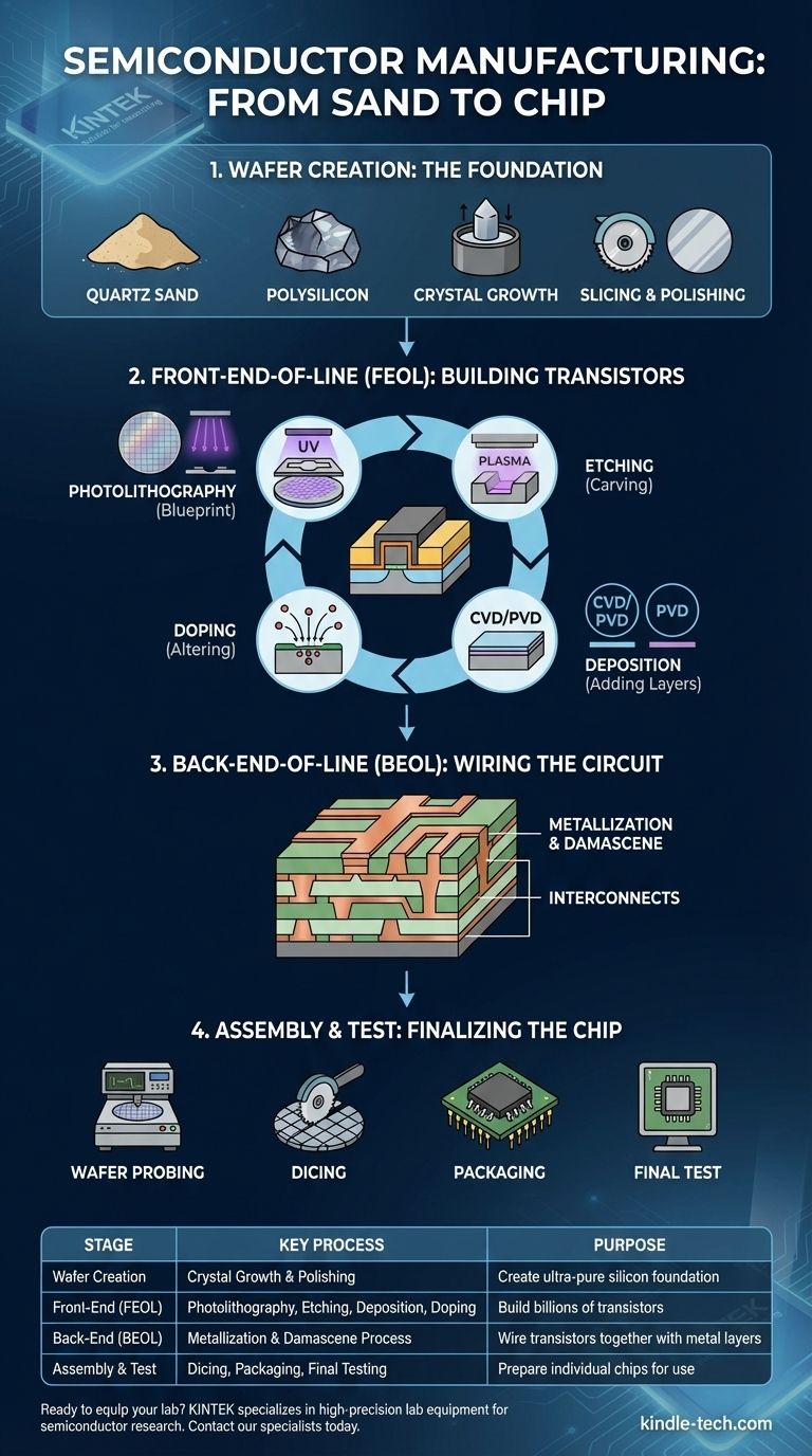
At its core, semiconductor manufacturing is a process of building a microscopic city of billions of electronic switches on a wafer of pure silicon. This is not a single action but a highly controlled sequence of hundreds of distinct steps, broadly divided into four main stages: creating the silicon wafer, fabricating the circuits on the wafer (front-end), wiring those circuits together (back-end), and finally, testing and packaging the finished chips. Each stage requires a level of precision that is among the most demanding in all of modern industry.
The central concept to grasp is that chipmaking is an iterative cycle of additive and subtractive processes. Layers of material, sometimes only atoms thick, are meticulously deposited onto a silicon wafer, patterned using light, and then selectively etched away to gradually form the billions of transistors that make up a modern integrated circuit.
From Sand to Silicon: Creating the Wafer
Before any circuit can be made, the foundation must be perfect. This foundation is a nearly flawless, ultra-pure disc of silicon called a wafer.
The Raw Material: Polysilicon
The process begins with quartz sand (silicon dioxide), which is heated and purified to produce metallurgical-grade silicon. This is then further refined into electronic-grade polysilicon, a material that is 99.9999999% pure. This extreme purity is non-negotiable, as even the slightest impurity can ruin a chip's electrical properties.
Growing the Ingot
This polysilicon is melted in a crucible. A tiny seed crystal is dipped into the molten silicon and slowly pulled upwards while rotating. As it is pulled, the molten silicon cools and solidifies, following the crystalline structure of the seed. This creates a large, single-crystal cylinder known as an ingot or "boule," which can be over two meters long and weigh hundreds of kilograms.
Slicing and Polishing
The cylindrical ingot is then sliced into very thin discs using a diamond-tipped saw. These raw discs, known as wafers, are ground and polished to a mirror-like, defect-free surface. A typical wafer is less than a millimeter thick but must be perfectly flat.
The Core of Chipmaking: Front-End-of-Line (FEOL)
This is where the transistors—the fundamental on/off switches of a chip—are constructed directly on the surface of the silicon wafer. This happens through a repeating cycle of four key processes.
Step 1: Photolithography (The Blueprint)
Photolithography is the single most critical step in chipmaking. A layer of light-sensitive material, called photoresist, is coated onto the wafer. A mask, which acts like a stencil containing the blueprint for one layer of the circuit, is positioned above the wafer. A specific wavelength of light (often deep ultraviolet, or DUV/EUV) is then projected through the mask, altering the chemical structure of the exposed photoresist.
Step 2: Etching (Carving the Pattern)
The wafer is then exposed to chemicals or plasma that remove the softened photoresist. This leaves a patterned layer of hardened photoresist, protecting some areas of the wafer while exposing others. In the etching process, a gas (dry etch) or liquid (wet etch) is used to remove the material from the exposed areas, carving the circuit pattern into the underlying layer.
Step 3: Deposition (Adding New Layers)
After etching, new layers of material are added to the wafer. Chemical Vapor Deposition (CVD) is a process where gases react to form a solid film on the wafer, used for creating insulating (dielectric) layers. Physical Vapor Deposition (PVD), or sputtering, bombards a target material with ions, knocking atoms loose that then deposit onto the wafer, often used for metal layers.
Step 4: Doping (Altering Conductivity)
To make a transistor work, the electrical properties of the silicon itself must be modified. This is done through ion implantation, a process where a high-energy particle accelerator shoots specific ions (like boron or phosphorus) into the silicon wafer. This "doping" creates the negative-type (N-type) and positive-type (P-type) regions that allow a transistor to switch on and off.
This cycle of lithography, etch, deposition, and doping is repeated hundreds of times to build the complex, three-dimensional structures of modern transistors.
Connecting the Transistors: Back-End-of-Line (BEOL)
Once the billions of transistors are formed in the FEOL stage, they must be wired together. This "wiring," known as the interconnect, is a dense, multi-layered grid of copper or aluminum pathways built on top of the transistors.
The Metallization Process
The BEOL process closely mirrors the FEOL but focuses on creating conductive pathways instead of transistors. A layer of insulating material is deposited, and then lithography and etching are used to create trenches and vias (vertical connections) where the wires will go.
Building the Wiring Layers
These trenches are then filled with copper in a process called damascene. The excess copper on the surface is polished away, leaving a perfectly flat layer with inlaid copper wiring. This process is repeated to build up a complex "highway system" of 10-20 layers of wiring that connects all the individual transistors into a functioning circuit.
Understanding the Trade-offs and Challenges
The semiconductor manufacturing process is defined by its extreme challenges. Success is measured by the ability to overcome them.
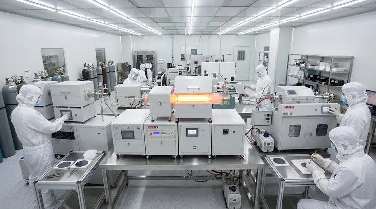
The Tyranny of Cleanliness
A modern transistor is so small that a single speck of dust is like a giant boulder, capable of shorting a circuit and destroying an entire chip. This is why chips are made in cleanrooms, facilities that are thousands of times cleaner than a surgical operating room. Workers must wear head-to-toe "bunny suits" to prevent contamination.
The Pursuit of Smaller Nodes
The industry's progress is driven by making transistors smaller, a trend described by Moore's Law. These "process nodes" (e.g., 7nm, 5nm) refer to the scale of the features on the chip. As features shrink, physical challenges like quantum tunneling—where electrons leak through insulators—become significant, requiring new materials and transistor designs (like FinFETs).
Yield: The Ultimate Metric of Success
Yield is the percentage of working chips per wafer. Because the process has hundreds of steps, a tiny error at any stage can create a defect. A yield of 90% may sound high, but it means 10% of the incredibly expensive production is worthless. Improving yield by even 1-2% can result in millions of dollars in additional revenue.
Finalizing the Chip: Assembly and Test
After hundreds of steps, the wafer holds hundreds or thousands of individual chips, known as dies.
Wafer Testing and Dicing
First, automated probes test each individual die on the wafer to identify which ones are functional. The wafer is then cut into individual dies with a diamond saw in a process called dicing.
Packaging and Final Test
The functional dies are then sent for packaging. The tiny, fragile silicon die is mounted onto a substrate and encapsulated in a protective plastic or ceramic housing. This package provides the metal pins or pads that connect the chip to the outside world. After packaging, the chip undergoes a final, rigorous test before it is shipped.
Why This Process Matters
Understanding the fundamentals of chip fabrication provides crucial context for the entire technology landscape.
- If your primary focus is engineering or research: Recognize that the iterative cycle of lithography, etch, deposition, and doping is the fundamental building block of all modern electronics.
- If your primary focus is business or investment: Understand that yield, the immense capital cost of a fabrication plant (fab), and the relentless race to smaller process nodes are the primary drivers of market competition and supply chain dynamics.
- If your primary focus is technology in general: Appreciate that the smartphone in your hand or the server running in the cloud is the result of one of the most complex, precise, and expensive manufacturing processes ever developed by humankind.
Ultimately, the digital world is built not just on clever software, but on a physical foundation of applied physics and manufacturing precision at an almost unimaginable scale.
Summary Table:
| Stage | Key Process | Purpose |
|---|---|---|
| Wafer Creation | Crystal Growth & Polishing | Create ultra-pure silicon foundation |
| Front-End (FEOL) | Photolithography, Etching, Deposition, Doping | Build billions of transistors |
| Back-End (BEOL) | Metallization & Damascene Process | Wire transistors together with metal layers |
| Assembly & Test | Dicing, Packaging, Final Testing | Prepare individual chips for use |
Ready to equip your lab for semiconductor research or production? KINTEK specializes in high-precision lab equipment and consumables essential for semiconductor manufacturing processes, including deposition systems, etching tools, and wafer handling solutions. Our expertise ensures the reliability and purity your work demands. Contact our specialists today to discuss how we can support your laboratory's specific needs in the semiconductor industry.
Visual Guide
Related Products
- Optical Window Glass Substrate Wafer Quartz Plate JGS1 JGS2 JGS3
- Customizable PTFE Wafer Carriers for Semiconductor and Lab Applications
- Versatile PTFE Solutions for Semiconductor and Medical Wafer Processing
- Silicon Carbide (SIC) Ceramic Sheet Wear-Resistant Engineering Advanced Fine Ceramics
- Custom PTFE Wafer Holders for Lab and Semiconductor Processing
People Also Ask
- Can quartz glass be heated? Mastering High-Temperature Applications with Quartz
- What is the maximum temperature for quartz windows? Ensure Long-Term Reliability and Avoid Devitrification
- What are the uses of quartz glass? Essential for Extreme-Temperature and UV Applications
- What is the working temperature of quartz glass? Master Its High-Temp Limits & Applications
- What is optical quartz? The Ultimate Material for UV and High-Temp Optics