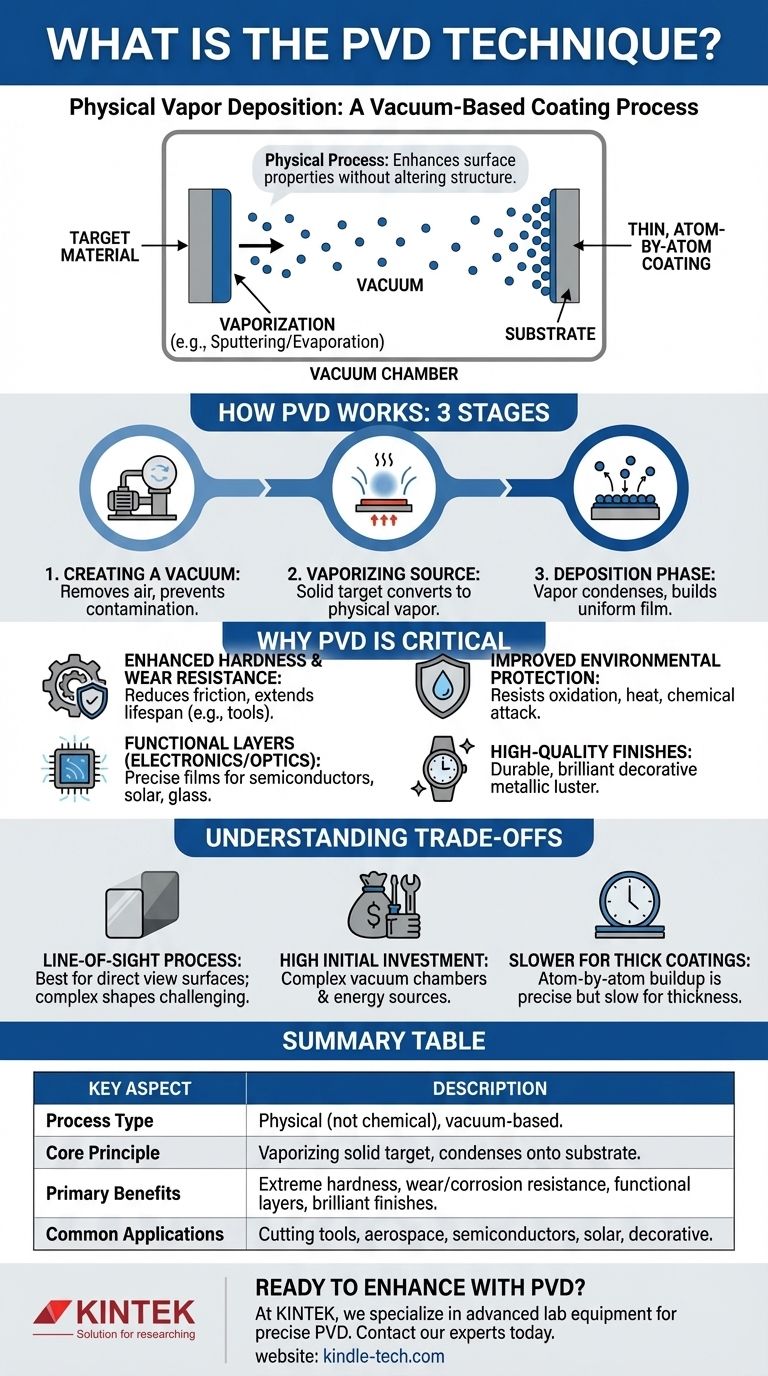
In essence, Physical Vapor Deposition (PVD) is a vacuum-based coating process used to apply extremely thin, high-performance films onto a surface. It works by transforming a solid source material into a vapor, which then travels through a vacuum chamber and condenses onto the target object. This builds the new coating one atom at a time, resulting in a pure, uniform, and highly adherent layer.
The critical distinction of PVD is that it is a physical process, not a chemical one. Think of it as a highly controlled "spray painting" with atoms, used to fundamentally enhance a material's surface properties without altering its underlying structure.
How PVD Works: The Core Principle
To understand PVD, it's best to break it down into its three essential stages. The entire process takes place under a very low-pressure (high vacuum) environment.
Step 1: Creating a Vacuum
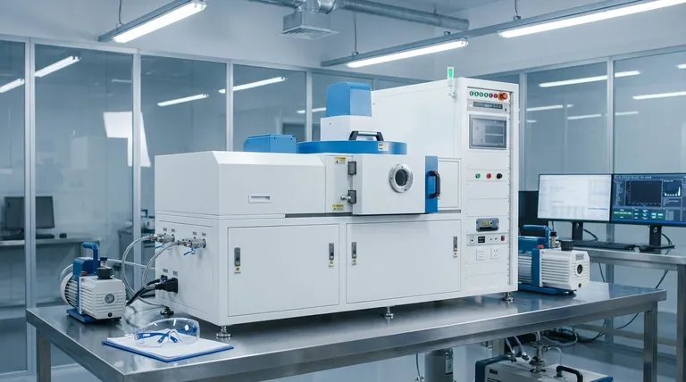
The process must occur inside a sealed vacuum chamber. Removing nearly all the air is critical to prevent contamination and to allow the vaporized coating atoms to travel from the source to the substrate without colliding with other particles.
Step 2: Vaporizing the Source Material
A pure, solid source material, known as the "target," is converted into a vapor. This is the "physical vapor" part of the name. Common methods include high-temperature evaporation or bombarding the target with high-energy ions (a process called sputtering).
Step 3: The Deposition Phase
The vaporized atoms travel in a straight line through the vacuum chamber and condense onto the surface of the substrate. This slow, atom-by-atom buildup creates an extremely thin, dense, and uniform film that is mechanically bonded to the surface.
Why PVD is a Critical Manufacturing Tool
PVD is not just a coating method; it's a technique for imparting new properties to a material's surface. Its applications are driven by the specific functional improvements it delivers.
Enhancing Hardness and Wear Resistance
PVD is widely used to apply ultra-hard coatings to cutting tools, engine components, and other items. These layers significantly reduce friction and improve resistance to wear and abrasion, extending the product's lifespan.
Improving Environmental Protection
The dense films created by PVD act as a powerful barrier. They can make a substrate highly resistant to oxidation (rust), high temperatures, and chemical attack, which is critical in aerospace and industrial applications.
Creating Functional Electronic and Optical Layers
The precision of PVD is essential in high-tech manufacturing. It is used to create the specific thin-film layers required for semiconductor devices, thin-film solar panels, and specialized low-reflection glass coatings.
Achieving High-Quality Finishes
PVD provides a durable and brilliant finish for decorative items. Because the coating perfectly mirrors the texture of the underlying surface, it can produce a bright metallic luster on plastics or metals without requiring post-polishing.
Understanding the Trade-offs
While powerful, PVD is not a universal solution. Understanding its inherent characteristics is key to using it effectively.
A Line-of-Sight Process
Because the vaporized atoms travel in a straight line, PVD is most effective at coating surfaces with a direct line of sight to the source material. Coating complex, three-dimensional shapes with deep recesses or internal channels can be challenging.
Requires High Initial Investment
The equipment required for PVD—specifically the vacuum chambers and the high-energy sources needed for vaporization—is complex and represents a significant capital investment.
Slower Deposition for Thick Coatings
Building a coating atom by atom is incredibly precise, but it can be slower than other methods like electroplating, especially if a very thick layer is required. PVD excels at creating films that are typically only a few microns thick.
When to Consider PVD for Your Project
The decision to use PVD should be based on the functional goal for your material's surface.
- If your primary focus is durability and wear resistance: PVD is an excellent choice for applying hard coatings that reduce friction and improve the lifespan of tools and components.
- If your primary focus is advanced electronics or optics: The precision of PVD makes it essential for creating the thin, functional films required in semiconductors, sensors, and solar panels.
- If your primary focus is a high-quality decorative finish: PVD provides a durable, brilliant coating on items like watches or fixtures that far surpasses traditional plating in toughness.
- If your primary focus is thermal or chemical protection: PVD can create powerful barrier layers that protect substrates from oxidation, high temperatures, and chemical corrosion.
Ultimately, PVD is the definitive technique for enhancing a material's surface properties without altering its fundamental composition.
Summary Table:
| Key Aspect | Description |
|---|---|
| Process Type | Physical (not chemical), vacuum-based |
| Core Principle | Vaporizing a solid target material, which then condenses atom-by-atom onto a substrate |
| Primary Benefits | Extreme hardness, wear resistance, corrosion/oxidation protection, functional electronic layers, brilliant decorative finishes |
| Common Applications | Cutting tools, aerospace components, semiconductors, solar panels, decorative hardware |
| Key Consideration | Line-of-sight process; best for surfaces with direct view of the source |
Ready to enhance your materials with high-performance PVD coatings?
At KINTEK, we specialize in providing advanced lab equipment and consumables for precise and reliable PVD processes. Whether you're developing wear-resistant tools, protective barriers, or sophisticated electronic components, our solutions are designed to meet the exacting demands of your laboratory.
Contact our experts today to discuss how KINTEK can support your PVD coating projects and help you achieve superior surface properties.
Visual Guide
Related Products
- RF PECVD System Radio Frequency Plasma-Enhanced Chemical Vapor Deposition RF PECVD
- Split Chamber CVD Tube Furnace with Vacuum Station Chemical Vapor Deposition System Equipment Machine
- Chemical Vapor Deposition CVD Equipment System Chamber Slide PECVD Tube Furnace with Liquid Gasifier PECVD Machine
- VHP Sterilization Equipment Hydrogen Peroxide H2O2 Space Sterilizer
- Molybdenum Tungsten Tantalum Special Shape Evaporation Boat
People Also Ask
- Why is PECVD environment friendly? Understanding the Eco-Friendly Benefits of Plasma-Enhanced Coating
- What are the advantages of PECVD? Enable Low-Temperature, High-Quality Thin-Film Deposition
- What are the applications of PECVD? Essential for Semiconductors, MEMS, and Solar Cells
- How does RF power create plasma? Achieve Stable, High-Density Plasma for Your Applications
- What is an example of PECVD? RF-PECVD for High-Quality Thin Film Deposition


