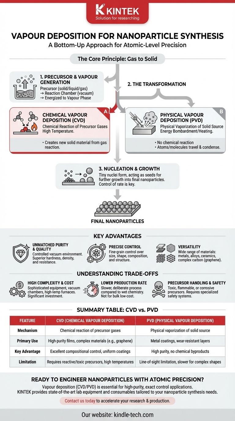
Vapour deposition for nanoparticle synthesis is a powerful "bottom-up" manufacturing technique where materials in a gaseous state are precisely converted into solid nanoparticles. This process allows for building materials atom by atom or molecule by molecule, resulting in exceptionally high purity and controlled structures. It is not a single method but a family of techniques, most commonly categorized as either Chemical Vapour Deposition (CVD) or Physical Vapour Deposition (PVD).
The core principle of vapour deposition is its unparalleled control. By manipulating gas-phase precursors in a controlled environment, you can dictate the final size, shape, composition, and crystalline structure of the nanoparticles with a precision that few other methods can match.
The Core Principle: Building from Gas to Solid
Vapour deposition works by taking a source material, converting it into a gas (vapour), and then inducing a change that causes it to condense back into a solid, but in the form of discrete nanoparticles.
From Precursor to Vapour
The process begins with a precursor material, which can be a solid, liquid, or gas that contains the atoms you want in your final nanoparticle. This precursor is introduced into a reaction chamber, typically under vacuum, and energized to create a vapour phase.
The Transformation: Chemical vs. Physical
This is the critical step where the gaseous atoms or molecules are transformed so they can become a solid. There are two primary pathways:
- Chemical Vapour Deposition (CVD): In CVD, the precursor gases undergo a chemical reaction (often triggered by high temperature) near a substrate. The reaction creates new, solid material that then forms nanoparticles. As the references note, all materials for the film come from this external gas source.
- Physical Vapour Deposition (PVD): In PVD, no chemical reaction occurs. A solid source material is physically bombarded with energy (e.g., with an ion beam in "sputtering" or heated in "evaporation") to release atoms into a vapour. This vapour then travels and condenses to form nanoparticles.
Nucleation and Growth
Once the solid material begins to form from the vapour, it doesn't appear all at once. Tiny clusters of atoms, called nuclei, form first. These nuclei then act as seeds for further growth, eventually developing into the final nanoparticles. Controlling the rate of nucleation versus the rate of growth is the key to controlling particle size.
Key Advantages of Vapour Deposition
The granular, atom-by-atom nature of this method provides several distinct advantages, making it essential for high-performance applications.
Unmatched Purity and Quality
Because the process occurs in a controlled vacuum environment using purified precursor gases, the resulting nanoparticles have extremely high purity. This leads to materials with superior hardness, excellent density, and greater resistance to damage compared to those made with other methods.
Precise Control Over Nanoparticle Properties
By carefully adjusting parameters like temperature, pressure, and gas composition, you gain fine-grained control over the final product. This allows you to dictate the nanoparticle's chemical composition, morphology (shape), crystal structure, and grain size with high fidelity.
Versatility in Materials and Substrates
Vapour deposition is not limited to one type of material. It can be used to create a vast range of nanoparticles, including pure metals, alloys, ceramics (like oxides and nitrides), and complex carbon structures like graphene. Furthermore, it has excellent "wrap-around" properties for uniformly coating complex 3D surfaces.
Understanding the Trade-offs
While powerful, vapour deposition is not a universal solution. Its precision comes with significant practical considerations.
High Equipment Complexity and Cost
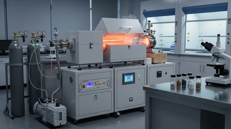
These methods require sophisticated and expensive equipment. A typical setup involves vacuum chambers, high-temperature furnaces, precise mass-flow controllers for gases, and extensive safety systems, representing a significant capital investment.
Lower Production Rate
Compared to "wet chemistry" methods (like sol-gel or precipitation) that can produce large batches of nanoparticles in a liquid solution, vapour deposition is generally a slower, more deliberate process. This makes it less suitable for applications requiring bulk quantities of material at low cost.
Precursor Handling and Safety
Many precursors used, particularly in CVD, are highly toxic, flammable, or corrosive. This necessitates specialized storage, handling procedures, and exhaust treatment systems to ensure operator and environmental safety.
Making the Right Choice for Your Goal
Selecting a synthesis method depends entirely on your project's end goal and constraints.
- If your primary focus is ultimate purity and perfect crystalline quality: Vapour deposition, especially CVD, is the superior choice for applications in high-performance electronics, advanced catalysts, or quantum dots.
- If your primary focus is coating a complex surface or depositing a pure metal: PVD is often the ideal method, commonly used for creating optical films, wear-resistant tool coatings, and biocompatible medical implants.
- If your primary focus is bulk production at the lowest possible cost: You should strongly consider alternative "wet chemical" synthesis methods, as they are generally more scalable and economical for large volumes.
Ultimately, vapour deposition empowers you to engineer materials from the ground up, offering atomic-level control as its defining advantage.
Summary Table:
| Feature | Chemical Vapour Deposition (CVD) | Physical Vapour Deposition (PVD) |
|---|---|---|
| Mechanism | Chemical reaction of precursor gases | Physical vaporization of solid source |
| Primary Use | High-purity films, complex materials (e.g., graphene) | Metal coatings, wear-resistant layers |
| Key Advantage | Excellent compositional control, uniform coatings | High purity, no chemical byproducts |
| Limitation | Requires reactive/toxic precursors, high temperatures | Line-of-sight limitation, slower for complex shapes |
Ready to Engineer Nanoparticles with Atomic Precision?
Vapour deposition techniques like CVD and PVD are essential for applications demanding the highest purity and exact control—from advanced electronics to durable coatings. At KINTEK, we specialize in providing state-of-the-art lab equipment and consumables tailored to your nanoparticle synthesis needs.
Whether you're developing next-generation catalysts, quantum dots, or specialized thin films, our expertise ensures you achieve reproducible, high-quality results.
Contact us today to discuss how our solutions can accelerate your research and production. Get in touch via our contact form and let’s build the future of materials, together.
Visual Guide
Related Products
- Chemical Vapor Deposition CVD Equipment System Chamber Slide PECVD Tube Furnace with Liquid Gasifier PECVD Machine
- RF PECVD System Radio Frequency Plasma-Enhanced Chemical Vapor Deposition RF PECVD
- 915MHz MPCVD Diamond Machine Microwave Plasma Chemical Vapor Deposition System Reactor
- HFCVD Machine System Equipment for Drawing Die Nano-Diamond Coating
- Customer Made Versatile CVD Tube Furnace Chemical Vapor Deposition Chamber System Equipment
People Also Ask
- Why is Chemical Vapor Deposition (CVD) equipment uniquely suited for constructing hierarchical superhydrophobic structures?
- What are the advantages of chemical vapor deposition? Achieve Superior Thin Films for Your Lab
- What is the chemical vapor deposition growth process? Build Superior Thin Films from the Atom Up
- What types of substrates are used in CVD to facilitate graphene films? Optimize Graphene Growth with the Right Catalyst
- What is plasma enhanced chemical vapor deposition PECVD equipment? A Guide to Low-Temperature Thin Film Deposition


