While numerous specialized methods exist, the most common techniques for measuring thin film thickness fall into three primary categories: optical analysis (like ellipsometry), physical measurement (like stylus profilometry), and high-resolution imaging (like electron microscopy). The methods mentioned in background materials—such as CVD and PVD—are deposition techniques used to create films, not measurement techniques used to characterize them.
The choice of a thin film measurement technique is not one-size-fits-all. It is a critical decision driven by the film's material properties (e.g., transparency, conductivity) and the specific requirements of the application, such as the need for destructive vs. non-destructive analysis.
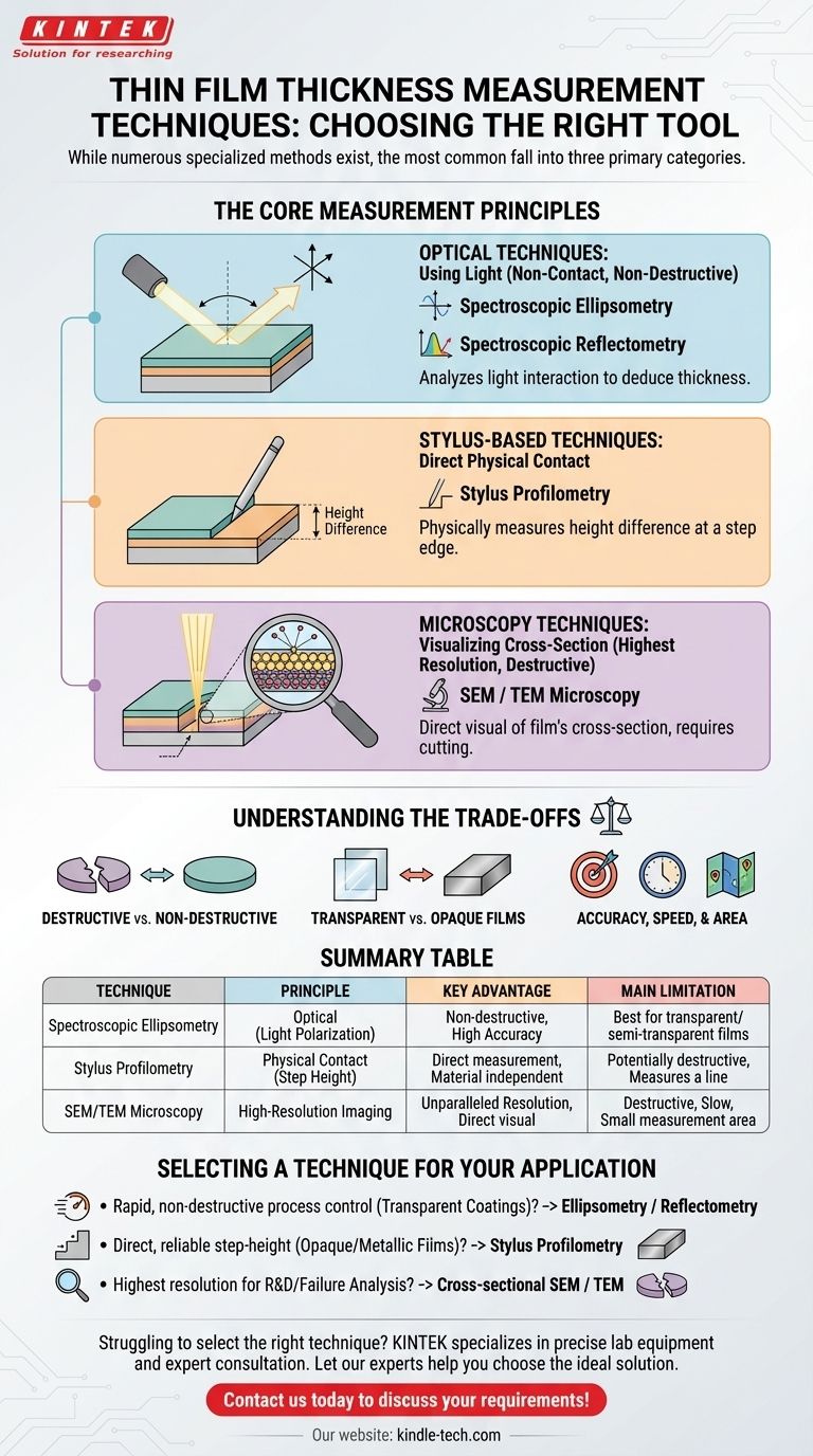
The Core Measurement Principles
To accurately control the function of a thin film, its thickness must be precisely measured. This is achieved through several distinct approaches, each with its own mechanism and ideal use case.
Optical Techniques: Using Light to Measure
Optical methods are powerful because they are non-contact and non-destructive. They analyze how light interacts with the thin film to deduce its thickness.
Spectroscopic Ellipsometry is a highly accurate optical technique. It measures the change in the polarization of light as it reflects off the thin film surface, providing precise thickness and optical constant data.
Spectroscopic Reflectometry is another common optical method. It measures the amount of light reflected from a film over a range of wavelengths, which can be used to calculate thickness.
Stylus-Based Techniques: Direct Physical Contact
This approach involves physically touching the surface to measure a height difference.
Stylus Profilometry is the most common direct-contact method. It works by dragging a fine-tipped stylus across a step edge from the substrate to the top of the thin film, physically measuring the height difference.
This technique is valued for its directness and its indifference to the optical properties of the film.
Microscopy Techniques: Visualizing the Cross-Section
For the highest possible resolution, microscopy techniques provide a direct visual of the film's cross-section.
Scanning Electron Microscopy (SEM) and Transmission Electron Microscopy (TEM) can image a prepared cross-section of the film. This allows for a direct visual measurement of thickness from the resulting image.
These methods offer unparalleled detail but are inherently destructive, as the sample must be physically cut to be viewed.
Understanding the Trade-offs
Selecting the right tool requires understanding the fundamental compromises between different methods. The ideal technique for one application may be entirely unsuitable for another.
Destructive vs. Non-Destructive
This is often the first and most critical consideration. Ellipsometry and reflectometry are non-destructive and can be used for in-line process monitoring on valuable samples.
In contrast, stylus profilometry can potentially scratch the surface, while cross-sectional SEM/TEM analysis requires destroying the sample entirely.
Transparent vs. Opaque Films
The optical properties of the film are a major deciding factor. Optical techniques like ellipsometry excel with films that are transparent or semi-transparent to the light being used.
For fully opaque films, such as thick metals, stylus profilometry is often a more reliable and straightforward choice because it does not depend on light transmission.
Accuracy, Speed, and Area
TEM offers the highest possible accuracy, capable of resolving individual atomic layers. However, it is slow, expensive, and measures only a minuscule point on the sample.
Optical techniques like reflectometry can be extremely fast, capable of mapping the thickness and uniformity across an entire large wafer in seconds. Stylus profilometry offers a balance, providing good accuracy over a scanned line.
Selecting a Technique for Your Application
Your final choice depends entirely on your material, budget, and measurement goal.
- If your primary focus is rapid, non-destructive process control of transparent optical coatings: Spectroscopic ellipsometry or reflectometry is the industry standard.
- If you need a direct, reliable physical measurement of a step-height on an opaque or metallic film: Stylus profilometry provides an unambiguous and trusted result.
- If you require the highest possible resolution for research, development, or failure analysis: Cross-sectional SEM or TEM is the definitive, albeit destructive, method.
Ultimately, understanding these core trade-offs empowers you to select the measurement technique that delivers the necessary accuracy without compromising your sample or your workflow.
Summary Table:
| Technique | Principle | Key Advantage | Main Limitation |
|---|---|---|---|
| Spectroscopic Ellipsometry | Optical (Light Polarization) | Non-destructive, High Accuracy | Best for transparent/semi-transparent films |
| Stylus Profilometry | Physical Contact (Step Height) | Direct measurement, Material independent | Potentially destructive, Measures a line |
| SEM/TEM Microscopy | High-Resolution Imaging | Unparalleled Resolution, Direct visual | Destructive, Slow, Small measurement area |
Struggling to select the right technique for your thin film analysis? The accuracy of your results depends on using the correct tool for your specific material and application. KINTEK specializes in providing precise lab equipment and expert consultation to meet your laboratory's thin film characterization needs. Let our experts help you choose the ideal solution to ensure accurate and reliable measurements. Contact us today to discuss your requirements and enhance your workflow!
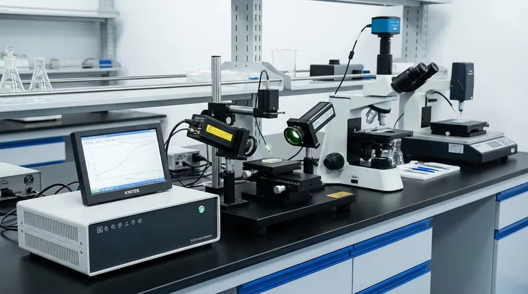
Visual Guide