Blog MPCVD Single Crystal Diamond Applications in Semiconductor and Optical Display Fields
MPCVD Single Crystal Diamond Applications in Semiconductor and Optical Display Fields

MPCVD Single Crystal Diamond Applications in Semiconductor and Optical Display Fields

1 month ago

Semiconductor Industry

Chip Substrate

Diamond materials, recognized as third-generation semiconductor materials, exhibit exceptional properties that make them highly suitable for various advanced electronic applications. These materials boast high thermal conductivity, which ensures efficient heat dissipation, critical for maintaining the performance and longevity of integrated circuit chips. Additionally, diamond's high breakdown field and high carrier mobility enable it to handle high-frequency and high-power operations with minimal energy loss, making it an ideal choice for cutting-edge electronic devices.

Moreover, the low dielectric constant of diamond materials reduces signal delay and power consumption, further enhancing their utility in ultra-high frequency high-power electronic devices. This combination of properties positions diamond substrates as a transformative material in the semiconductor industry, promising to drive innovation in integrated circuits and beyond.

Chip Heat Dissipation Materials

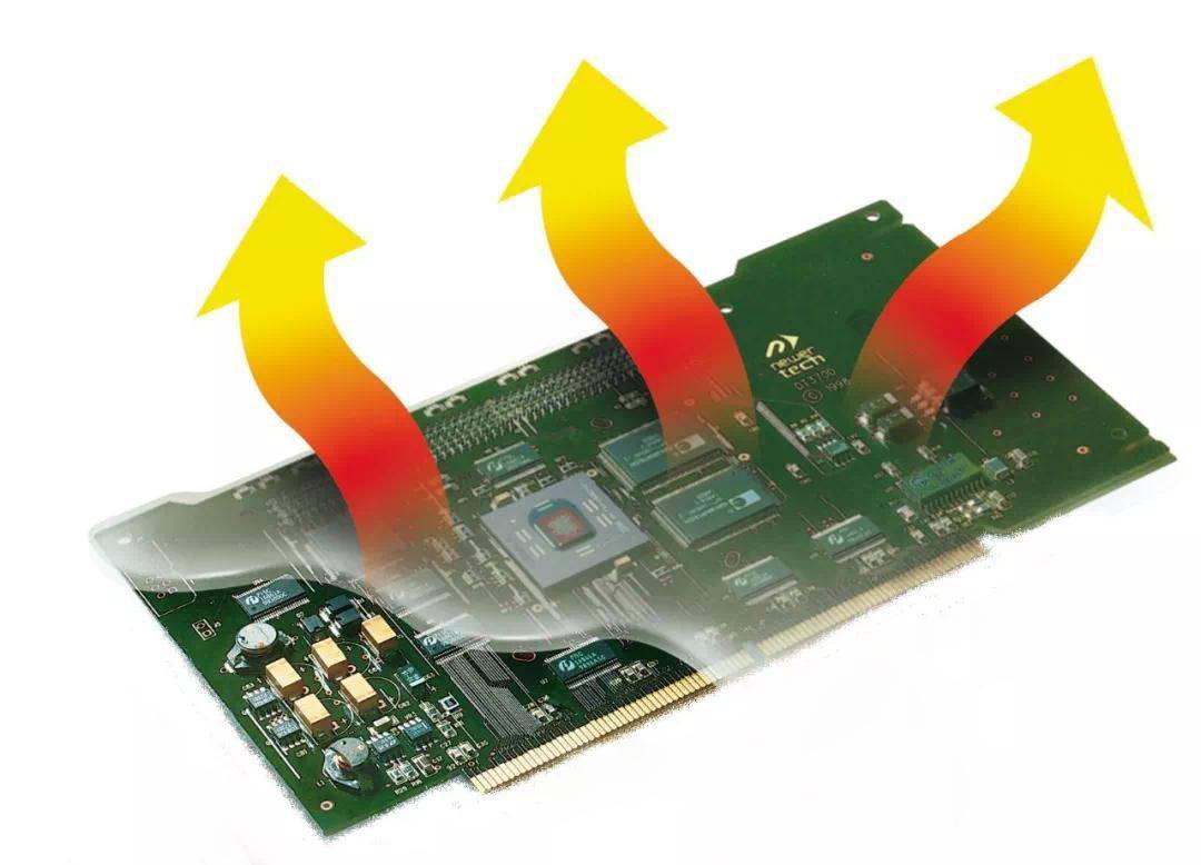
Monocrystalline diamond stands out as the most ideal material for heat dissipation in high-power, high-density devices due to its exceptional thermal conductivity. This property is crucial for maintaining optimal performance and longevity in advanced technologies such as 5G chips and laser diode arrays. The high thermal conductivity of monocrystalline diamond ensures that it can efficiently dissipate heat, preventing thermal degradation and enhancing the overall reliability of these devices.

In the realm of 5G technology, where chips operate at unprecedented speeds and power levels, the ability to manage heat is paramount. Monocrystalline diamond's superior thermal management capabilities make it an indispensable component in these high-performance systems. Similarly, in laser diode arrays, which are used in a variety of applications from telecommunications to medical devices, the efficient heat dissipation provided by monocrystalline diamond ensures stable and consistent operation.
Chip Heat Dissipation Materials

Moreover, the unique properties of monocrystalline diamond, including its high breakdown field and carrier mobility, further enhance its suitability for these applications. These attributes not only improve the thermal management but also contribute to the overall efficiency and performance of the devices. As the demand for faster, more powerful, and more compact electronic devices continues to grow, the role of monocrystalline diamond as a key heat dissipation material will become increasingly significant.

Optical Display Field

Cold Cathode Field Emission Display (FED)

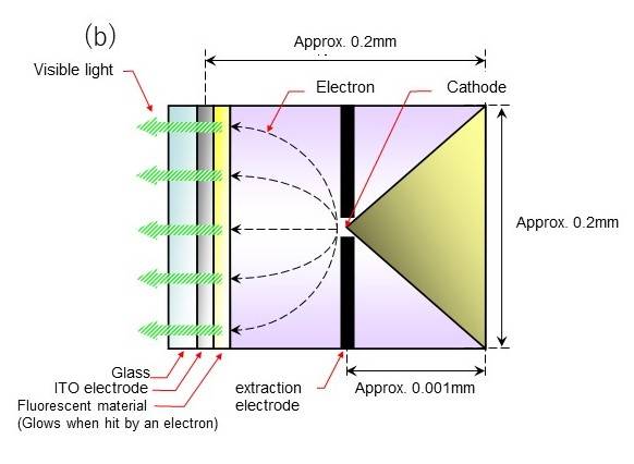
The Cold Cathode Field Emission Display (FED) stands as a pioneering technology in the realm of self-luminous flat-panel displays, leveraging the exceptional properties of single crystal diamond materials. This innovative display technology capitalizes on diamond's unparalleled optical, mechanical, thermal, and electrical characteristics to deliver a superior viewing experience.

One of the key advantages of FED is its remarkable brightness. The inherent transparency and high refractive index of single crystal diamond enable the creation of displays with unparalleled luminance, ensuring that images are vivid and clear even under direct sunlight. This makes FED ideal for applications requiring high visibility, such as outdoor digital signage and military equipment.
Cold Cathode Field Emission Display (FED)

In addition to brightness, FEDs offer exceptional grayscale and color fidelity. The precise control over electron emission in diamond-based FEDs allows for a wide range of grayscale levels, resulting in highly detailed and lifelike images. The material's ability to emit light across the visible spectrum ensures rich and accurate color reproduction, setting FED apart from traditional displays.

Resolution is another area where FED excels. The high electron mobility and low dielectric constant of single crystal diamond contribute to the creation of displays with ultra-high resolutions. This means that FEDs can render images with an extraordinary level of detail, making them suitable for applications demanding high-definition visuals, such as medical imaging and advanced gaming consoles.

Furthermore, FEDs boast an impressive response speed. The rapid electron emission and conduction properties of diamond enable these displays to switch between colors and grayscale levels at lightning speeds, ensuring smooth and fluid motion in fast-paced visuals. This makes FED an excellent choice for applications requiring rapid updates, such as high-speed data visualization and real-time simulations.

In summary, the Cold Cathode Field Emission Display (FED) leverages the exceptional properties of single crystal diamond to deliver a self-luminous flat-panel display with unparalleled advantages in brightness, grayscale, color, resolution, and response speed. This makes FED a promising technology for a wide range of applications, from consumer electronics to specialized industrial and military uses.

CONTACT US FOR A FREE CONSULTATION

KINTEK LAB SOLUTION's products and services have been recognized by customers around the world. Our staff will be happy to assist with any inquiry you might have. Contact us for a free consultation and talk to a product specialist to find the most suitable solution for your application needs!

Related Products

915MHz MPCVD Diamond Machine Microwave Plasma Chemical Vapor Deposition System Reactor

915MHz MPCVD Diamond Machine Microwave Plasma Chemical Vapor Deposition System Reactor

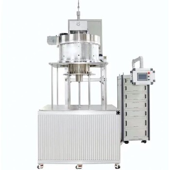
915MHz MPCVD Diamond Machine and its multi-crystal effective growth, the maximum area can reach 8 inches, the maximum effective growth area of single crystal can reach 5 inches. This equipment is mainly used for the production of large-size polycrystalline diamond films, the growth of long single crystal diamonds, the low-temperature growth of high-quality graphene, and other materials that require energy provided by microwave plasma for growth.

Microwave Plasma Chemical Vapor Deposition MPCVD Machine System Reactor for Lab and Diamond Growth

Microwave Plasma Chemical Vapor Deposition MPCVD Machine System Reactor for Lab and Diamond Growth

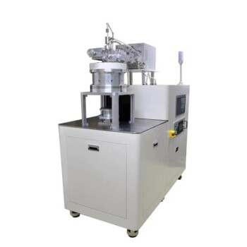
Get high-quality diamond films with our Bell-jar Resonator MPCVD machine designed for lab and diamond growth. Discover how Microwave Plasma Chemical Vapor Deposition works for growing diamonds using carbon gas and plasma.

Cylindrical Resonator MPCVD Machine System Reactor for Microwave Plasma Chemical Vapor Deposition and Lab Diamond Growth

Cylindrical Resonator MPCVD Machine System Reactor for Microwave Plasma Chemical Vapor Deposition and Lab Diamond Growth

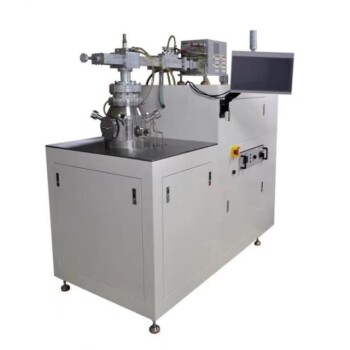
Learn about Cylindrical Resonator MPCVD Machine, the microwave plasma chemical vapor deposition method used for growing diamond gemstones and films in the jewelry and semi-conductor industries. Discover its cost-effective advantages over traditional HPHT methods.

Laboratory CVD Boron Doped Diamond Materials

Laboratory CVD Boron Doped Diamond Materials

CVD boron-doped diamond: A versatile material enabling tailored electrical conductivity, optical transparency, and exceptional thermal properties for applications in electronics, optics, sensing, and quantum technologies.

CVD Diamond for Thermal Management Applications

CVD Diamond for Thermal Management Applications

CVD diamond for thermal management: High-quality diamond with thermal conductivity up to 2000 W/mK, ideal for heat spreaders, laser diodes, and GaN on Diamond (GOD) applications.

Custom CVD Diamond Coating for Lab Applications

Custom CVD Diamond Coating for Lab Applications

CVD Diamond Coating: Superior Thermal Conductivity, Crystal Quality, and Adhesion for Cutting Tools, Friction, and Acoustic Applications

CVD Diamond Domes for Industrial and Scientific Applications

CVD Diamond Domes for Industrial and Scientific Applications

Discover CVD diamond domes, the ultimate solution for high-performance loudspeakers. Made with DC Arc Plasma Jet technology, these domes deliver exceptional sound quality, durability, and power handling.

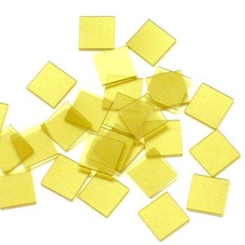
CVD Diamond Optical Windows for Lab Applications

CVD Diamond Optical Windows for Lab Applications

Diamond optical windows: exceptional broad band infrared transparency, excellent thermal conductivity & low scattering in infrared, for high-power IR laser & microwave windows applications.

HFCVD Machine System Equipment for Drawing Die Nano-Diamond Coating

HFCVD Machine System Equipment for Drawing Die Nano-Diamond Coating

The nano-diamond composite coating drawing die uses cemented carbide (WC-Co) as the substrate, and uses the chemical vapor phase method ( CVD method for short ) to coat the conventional diamond and nano-diamond composite coating on the surface of the inner hole of the mold.

CVD Diamond Cutting Tool Blanks for Precision Machining

CVD Diamond Cutting Tool Blanks for Precision Machining

CVD Diamond Cutting Tools: Superior Wear Resistance, Low Friction, High Thermal Conductivity for Non-Ferrous Materials, Ceramics, Composites Machining

CVD Diamond Wire Drawing Die Blanks for Precision Applications

CVD Diamond Wire Drawing Die Blanks for Precision Applications

CVD diamond wire drawing die blanks: superior hardness, abrasion resistance, and applicability in wire drawing various materials. Ideal for abrasive wear machining applications like graphite processing.

CVD Diamond Dressing Tools for Precision Applications

CVD Diamond Dressing Tools for Precision Applications

Experience the Unbeatable Performance of CVD Diamond Dresser Blanks: High Thermal Conductivity, Exceptional Wear Resistance, and Orientation Independence.

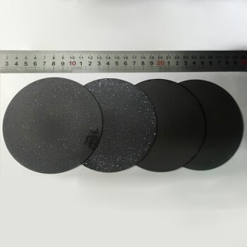
Silicon Carbide (SIC) Ceramic Sheet Flat Corrugated Heat Sink for Engineering Advanced Fine Ceramics

Silicon Carbide (SIC) Ceramic Sheet Flat Corrugated Heat Sink for Engineering Advanced Fine Ceramics

Silicon carbide (sic) ceramic heat sink not only does not generate electromagnetic waves, but also can isolate electromagnetic waves and absorb part of electromagnetic waves.

Advanced Engineering Fine Ceramics Aluminum Nitride (AlN) Ceramic Sheet

Advanced Engineering Fine Ceramics Aluminum Nitride (AlN) Ceramic Sheet

Aluminum nitride (AlN) has the characteristics of good compatibility with silicon. It is not only used as a sintering aid or reinforcing phase for structural ceramics, but its performance far exceeds that of alumina.

Optical Window Glass Substrate Wafer CaF2 Substrate Window Lens

Optical Window Glass Substrate Wafer CaF2 Substrate Window Lens

A CaF2 window is an optical window made of crystalline calcium fluoride. These windows are versatile, environmentally stable and resistant to laser damage, and they exhibit a high, stable transmission from 200 nm to about 7 μm.

High Purity Pure Graphite Crucible for Electron Beam Evaporation

High Purity Pure Graphite Crucible for Electron Beam Evaporation

A technology mainly used in the field of power electronics. It is a graphite film made of carbon source material by material deposition using electron beam technology.

Optical Window Glass Substrate Wafer Barium Fluoride BaF2 Substrate Window

Optical Window Glass Substrate Wafer Barium Fluoride BaF2 Substrate Window

BaF2 is the fastest scintillator, sought-after for its exceptional properties. Its windows and plates are valuable for VUV and infrared spectroscopy.


Leave Your Message