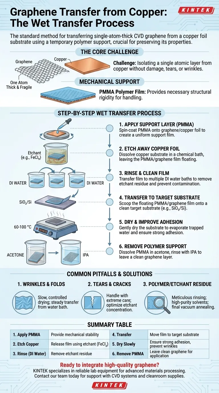
The standard method for transferring graphene from copper foil is a wet transfer process that uses a polymer film as a temporary mechanical support. This process involves coating the graphene with the polymer, chemically etching away the copper substrate, transferring the now-floating graphene/polymer film to a new substrate, and finally dissolving the polymer support to leave a clean graphene layer.
The core challenge of graphene transfer is not simply moving the material, but preserving its pristine, single-atom-thick structure. Success hinges on preventing tears, wrinkles, and chemical contamination, as any defect will degrade the exceptional properties you seek to harness.
The Challenge: Isolating a Single Atomic Layer
Graphene grown via Chemical Vapor Deposition (CVD) on copper foil is of high quality, but it is chemically bonded and physically adhered to that metal growth substrate. The goal is to move this incredibly thin film—just one atom thick—to a new, useful substrate (like silicon dioxide) without destroying it.
The Role of Mechanical Support
A freestanding sheet of graphene is far too fragile to handle on a macroscopic scale. It would immediately fold, tear, and collapse.
To prevent this, a support layer, typically a polymer like PMMA (Poly(methyl methacrylate)), is coated on top of the graphene before the transfer process begins. This polymer film provides the necessary structural rigidity to handle the graphene sheet safely.
The Standard Wet Transfer Process: A Step-by-Step Guide
This procedure is the workhorse of academic labs and industrial R&D for moving CVD graphene.
Step 1: Applying the Support Layer
The first step is to create the temporary support structure. A solution of PMMA dissolved in a solvent (like anisole) is applied to the graphene/copper foil.
The most common method is spin-coating, which creates a uniform, thin film of PMMA across the entire surface. The thickness of this layer is a key parameter; a thicker layer offers more support but can be harder to remove cleanly later.
Step 2: Etching Away the Copper Foil
With the graphene protected, the copper substrate can be removed. The PMMA-coated foil is placed in a chemical bath that dissolves copper but does not affect graphene or PMMA.
Common etchants include ferric chloride (FeCl₃) or ammonium persulfate ((NH₄)₂S₂O₈). As the copper dissolves away over several hours, the transparent PMMA/graphene film is released and is left floating on the surface of the etchant solution.
Step 3: Rinsing and Cleaning the Graphene Film
This is a critical step for ensuring high-quality graphene. The floating film will be covered in etchant residue, which, if not removed, will contaminate the final graphene layer and ruin its electronic properties.
The PMMA/graphene film is carefully transferred, often multiple times, to baths of deionized (DI) water to rinse away any residual chemicals.
Step 4: Transferring to the Target Substrate
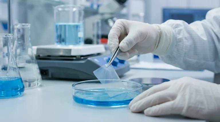
Once clean, the film is ready to be moved to its final destination. A target substrate, such as a silicon wafer with a silicon dioxide layer (SiO₂/Si), is submerged into the DI water bath at an angle.
The substrate is then slowly lifted out, "scooping" the floating PMMA/graphene film out of the water. Surface tension helps the film adhere smoothly to the new substrate.
Step 5: Drying and Improving Adhesion
The substrate with the wet film is now gently dried. This is often done by leaving it in a low-humidity environment or by gentle heating on a hot plate at a low temperature (e.g., 60-100 °C).
This slow drying process is crucial to evaporate any trapped water between the graphene and the substrate, ensuring intimate contact and strong adhesion while preventing wrinkles.
Step 6: Removing the Polymer Support
The final step is to remove the PMMA support layer, leaving only the pure graphene. The substrate is submerged in a solvent that dissolves PMMA, most commonly acetone.
After the PMMA has dissolved, the substrate is typically rinsed in isopropyl alcohol (IPA) to remove any final acetone or polymer residue. After a final gentle drying, the graphene transfer is complete.
Common Pitfalls and How to Avoid Them
The quality of your final device depends entirely on the quality of the transfer. Understanding what can go wrong is key to success.
Wrinkles and Folds
These are often caused by trapped water or uneven stress during the drying phase. To avoid them, ensure the drying process is slow and uniform. Pulling the film from the water bath at a steady, controlled pace is also critical.
Tears and Cracks
Mechanical stress is the enemy of a single-atom-thick film. Handle the floating film with extreme care during the rinsing steps. Using an overly aggressive etchant can also create pinholes in the copper that lead to tears, so optimizing the etchant concentration is important.
Polymer and Etchant Residue
This is the most common and insidious problem, as the residue is often invisible but dramatically degrades graphene's electrical performance. The solution is meticulous cleaning. Use multiple, fresh DI water baths for rinsing and high-purity solvents for polymer removal. For high-performance applications, a final vacuum annealing step (heating in a vacuum) can help remove stubborn residue.
Making the Right Choice for Your Goal
The "best" transfer method is the one that meets the needs of your application.
- If your primary focus is maximum electronic performance: Prioritize cleanliness above all. Use multiple rinsing steps, high-purity solvents, and consider a final vacuum annealing to achieve a pristine graphene surface.
- If your primary focus is large-area structural integrity: Use a slightly thicker PMMA support layer for better mechanical stability and ensure a very slow, controlled drying process to minimize wrinkles and tears.
- If your primary focus is speed and throughput for initial testing: You can use a more concentrated etchant to speed up copper removal, but be aware that this may slightly compromise the quality and introduce more defects.
Mastering the transfer process is the foundational skill required to unlock the transformative potential of graphene in any application.
Summary Table:
| Step | Key Action | Purpose |
|---|---|---|
| 1 | Apply PMMA Support Layer | Provide mechanical stability for handling |
| 2 | Etch Copper Substrate | Release graphene/PMMA film using FeCl₃ or (NH₄)₂S₂O₈ |
| 3 | Rinse in DI Water | Remove etchant residue to prevent contamination |
| 4 | Transfer to Target Substrate | Scoop film onto SiO₂/Si or other useful substrate |
| 5 | Dry Slowly | Ensure strong adhesion and prevent wrinkles |
| 6 | Remove PMMA with Acetone | Leave clean graphene layer for application |
Ready to integrate high-quality graphene into your research or production? KINTEK specializes in providing reliable lab equipment and consumables tailored for advanced materials processing, including CVD systems and cleanroom supplies. Whether you're optimizing graphene transfer for electronics or scaling up for industrial applications, our expertise ensures you have the right tools for success. Contact our team today to discuss how we can support your laboratory's innovation goals!
Visual Guide
Related Products
- Laboratory CVD Boron Doped Diamond Materials
- CVD Diamond Wire Drawing Die Blanks for Precision Applications
- CVD Diamond for Thermal Management Applications
- CVD Diamond Dressing Tools for Precision Applications
- Custom CVD Diamond Coating for Lab Applications
People Also Ask
- Are CVD diamonds synthetic? Discover the Truth About Lab-Grown Diamonds
- How much cheaper are CVD diamonds? Save 20-30% on a Genuine Diamond
- What materials are CVD deposition? From Semiconductors to Super-Hard Coatings
- What is the purpose of performing anodic polarization on BDD electrodes? Ensure Accurate & Reproducible Research Results
- What are the applications of CVD diamonds? From Jewelry to High-Tech Tools


