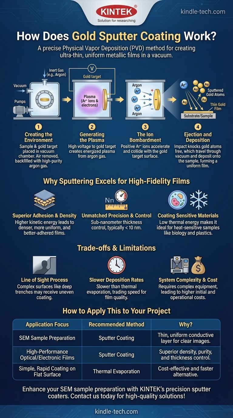
At its core, gold sputter coating is a physical vapor deposition (PVD) method used to create an ultra-thin, uniform metallic film. In a vacuum chamber, a high-voltage plasma is generated using an inert gas like argon. The energized argon ions are accelerated into a solid gold target, physically knocking gold atoms off its surface. These dislodged atoms then travel through the vacuum and deposit onto the substrate, forming a highly consistent and well-adhered coating.
Sputter coating is not merely about applying a layer of gold; it's a precision engineering process. It addresses the fundamental need for high-quality, dense, and exceptionally thin conductive films, particularly for applications like preparing non-conductive samples for high-resolution scanning electron microscopy (SEM).
The Sputtering Process: A Step-by-Step Breakdown
To truly understand how sputter coating works, it's best to visualize it as a controlled, atomic-level sandblasting process happening inside a vacuum. Each step is critical for the final quality of the film.
Step 1: Creating the Environment
First, the sample (or substrate) and the sputtering target (a piece of solid gold) are placed inside a sealed vacuum chamber. The chamber is evacuated to remove air and impurities, which could otherwise contaminate the film.
Once a high vacuum is achieved, the chamber is backfilled with a small, controlled amount of a high-purity inert gas, most commonly argon.
Step 2: Generating the Plasma
A strong negative electrical voltage is applied to the gold target. This high voltage strips electrons from the argon atoms, creating a mixture of positive argon ions (Ar+) and free electrons.
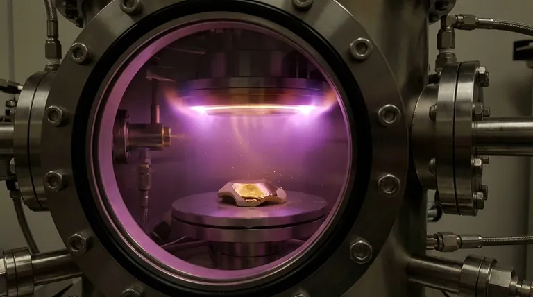
This energized, ionized gas is known as a plasma, which is often visible as a characteristic purple or pink glow.
Step 3: The Ion Bombardment
The positively charged argon ions are powerfully attracted and accelerated toward the negatively charged gold target.
They collide with the surface of the target with significant kinetic energy. This is a purely physical, momentum-transfer process.
Step 4: Ejection and Deposition
The impact of an argon ion has enough force to knock one or more gold atoms completely free from the target. This is the "sputtering" effect.
These sputtered gold atoms travel in a straight line through the low-pressure argon environment until they strike a surface—including your sample. Upon arrival, they condense and build up, atom by atom, to form a thin, continuous film.
Why Sputtering Excels for High-Fidelity Films
Sputtering is often preferred over simpler methods like thermal evaporation because of the superior characteristics of the resulting film. The energy of the process directly translates to higher quality.
Superior Film Adhesion and Density
Sputtered atoms arrive at the substrate with significantly more kinetic energy than evaporated atoms. This higher energy promotes better surface mobility and results in a denser, more uniform film with stronger adhesion to the sample.
Unmatched Precision and Control
The thickness of the sputtered film can be controlled with high precision. By managing the gas pressure, input current, and deposition time, it's possible to create films with sub-nanometer accuracy, often less than 10 nm thick.
Coating Sensitive and Complex Materials
While the plasma itself generates heat, the sputtered atoms have very low thermal energy. This makes the process ideal for coating heat-sensitive materials, such as biological samples or plastics, without causing thermal damage.
The process can also effectively coat complex, three-dimensional surfaces, which is critical for preparing irregularly shaped specimens for SEM analysis.
Understanding the Trade-offs and Limitations
No technique is perfect. Being a trusted technical advisor means acknowledging the limitations of sputter coating so you can make an informed decision.
It Is a "Line of Sight" Process
Sputtered atoms travel in straight lines from the target to the substrate. This means that deep trenches, undercuts, or shadowed areas on a complex sample may receive a thinner coating or no coating at all.
Slower Deposition Rates
Generally, sputtering is a slower process compared to thermal evaporation. The trade-off is speed for quality; achieving a dense, well-adhered film takes more time.
System Complexity and Cost
A sputter coater is a more complex piece of equipment than a thermal evaporator. It requires a robust vacuum system, precise gas flow controllers, and a high-voltage power supply, leading to higher initial and operational costs.
How to Apply This to Your Project
Your choice of coating method depends entirely on the requirements of your final application.
- If your primary focus is preparing non-conductive samples for SEM: Sputter coating is the industry standard, providing the thin, uniform conductive layer essential for preventing charge buildup and achieving clear, high-resolution images.
- If your primary focus is creating high-performance optical or electronic films: The superior density, purity, and thickness control of sputtering are non-negotiable for producing reliable and consistent device performance.
- If your primary focus is simple, rapid coating on a flat surface: Thermal evaporation may be a more cost-effective and faster alternative, assuming you can tolerate its limitations in film density and adhesion.
Understanding these core principles allows you to select the deposition technique that best aligns with your project's specific demands for quality, precision, and efficiency.
Summary Table:
| Aspect | Key Detail |
|---|---|
| Process Type | Physical Vapor Deposition (PVD) |
| Primary Use | Creating conductive layers for SEM on non-conductive samples |
| Key Advantage | Produces dense, uniform films with excellent adhesion |
| Typical Thickness | Less than 10 nm, with sub-nanometer control |
| Ideal For | Heat-sensitive materials, complex 3D surfaces |
Ready to enhance your SEM sample preparation with precision gold sputter coating? KINTEK specializes in high-quality lab equipment and consumables, providing reliable sputter coaters that deliver uniform, ultra-thin conductive films essential for clear, high-resolution imaging. Our solutions are designed for laboratories that demand accuracy and consistency. Contact us today to discuss how our sputter coating systems can meet your specific research or quality control needs!
Visual Guide
Related Products
People Also Ask
- What materials are used in electron beam evaporation? Master High-Purity Thin Film Deposition
- What is e-beam evaporation? Achieve High-Purity Thin Film Deposition for Your Lab
- How is an electron beam evaporator cooled during deposition? Essential Thermal Management for Stable Processes
- What is the current of e-beam evaporation? A Guide to High-Purity Thin Film Deposition
- What is the voltage of e-beam evaporation? Achieve Precise Thin-Film Deposition
