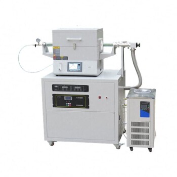
Plasma-Enhanced Chemical Vapor Deposition (PECVD) overcomes the primary thermal barrier associated with creating silicon carbide films. By utilizing high-energy plasma rather than relying solely on thermal energy to dissociate gaseous precursor molecules, PECVD equipment allows the necessary chemical reactions to occur at significantly reduced temperatures. This capability is the specific mechanism that enables the deposition of robust Silicon Carbide (SiC) thin films onto thermally sensitive substrates, such as polymers or low-melting-point semiconductors, which would melt or degrade under traditional processing conditions.
Core Takeaway: Traditional Chemical Vapor Deposition (CVD) often requires temperatures exceeding 1000°C to deposit silicon carbide. PECVD circumvents this by substituting thermal energy with electromagnetic energy (plasma) to activate chemical precursors. This allows advanced ceramic coatings to be applied to delicate substrates, unlocking critical applications in flexible electronics and biomedical microsensors.
The Energy Substitution Mechanism
Replacing Heat with Electron Impact
In standard thermal CVD, the energy required to break chemical bonds and initiate deposition comes entirely from heat. For materials like Silicon Carbide (SiC), this often requires substrate temperatures around 1050°C.
PECVD equipment fundamentally changes this energy equation. Instead of heating the entire chamber to these extreme temperatures, the system uses an electrical field to generate a plasma.
The Role of Reactive Radicals
Within the plasma, energetic electrons collide with the reactant and dilution gases. These collisions ionize or dissociate the gas molecules, creating highly reactive species known as radicals.
Because these radicals are already chemically active, they can react on the sample's surface to form a thin film without requiring the substrate itself to provide the massive thermal energy usually needed to trigger the reaction.
Inside the Process Chamber
Uniform Gas Distribution
To ensure the SiC film is consistent, reactant gases are introduced through a shower head. This is a perforated metal plate located directly above the sample which ensures even distribution of the gas mixture.
RF Potential and Plasma Generation
The equipment applies a Radio Frequency (RF) potential to this shower head. This electrical potential is the driving force that ignites and sustains the plasma between the shower head and the grounded substrate.
Surface Reaction Dynamics
Once the reactive radicals are generated by the plasma, they adsorb onto the substrate surface. The chemical reaction that creates the solid SiC film occurs here. Crucially, because the precursors were "pre-broken" by the plasma, the substrate can remain at a significantly lower temperature while still achieving successful deposition.
Expanding Application Horizons
Enabling Flexible Electronics
The primary advantage of this low-temperature capability is material compatibility. It allows engineers to deposit hard, chemically inert SiC coatings onto polymers and plastics.
This is essential for the manufacturing of flexible electronics, where the substrate must remain pliable and intact throughout the deposition process.
Biomedical Implications
This technology also facilitates the creation of biomedical microsensors. These devices often require biocompatible coatings like SiC but are built on delicate structures that cannot withstand the harsh environment of a standard thermal CVD furnace.
Understanding the Trade-offs
Equipment Complexity
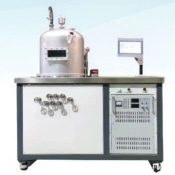
While PECVD lowers the thermal budget, it increases the hardware complexity. The requirement for RF generators, vacuum systems, and precise plasma control adds variables to the process that do not exist in simpler thermal evaporation methods.
Material Properties vs. Temperature
While PECVD allows for deposition at lower temperatures, the microstructure of the resulting film may differ from that produced by high-temperature thermal CVD.
High-temperature processes (like the 1050°C standard) generally produce highly dense, microstructurally uniform coatings. When moving to lower-temperature PECVD, parameters must be tuned carefully to ensure the film maintains the necessary adhesion and density for the intended application.
Making the Right Choice for Your Goal
To determine if PECVD is the correct approach for your silicon carbide application, consider the thermal constraints of your base material.
- If your primary focus is Substrate Integrity: Choose PECVD if you are working with polymers, flexible substrates, or chemically sensitive biosensors that cannot survive temperatures above 300-400°C.
- If your primary focus is Microstructural Density: Evaluate if a standard thermal CVD process is viable, provided your substrate is heat-resistant (e.g., graphite or high-temperature ceramics), as this may yield a denser coating.
- If your primary focus is Uniformity on Complex Geometries: Ensure your PECVD configuration utilizes a shower head distribution system to guarantee consistent radical delivery across the wafer surface.
PECVD is the technological bridge that allows the durability of advanced ceramics to be integrated into the delicate world of soft materials and next-generation electronics.
Summary Table:
| Feature | Thermal CVD | PECVD (Plasma-Enhanced) |
|---|---|---|
| Energy Source | Thermal Energy (Heat) | Electromagnetic Energy (Plasma) |
| Typical Temperature | > 1000°C | 200°C - 400°C |
| Substrate Compatibility | Heat-resistant (Graphite, Ceramics) | Thermally sensitive (Polymers, Plastics) |
| Key Mechanism | Thermal dissociation of gases | Electron impact & radical generation |
| Primary Application | Industrial coatings, dense ceramics | Flexible electronics, biomedical sensors |
Elevate Your Thin Film Research with KINTEK
Don't let thermal constraints limit your innovation. KINTEK specializes in advanced laboratory equipment, offering high-performance PECVD systems designed to deliver robust Silicon Carbide coatings without compromising sensitive substrates.
Whether you are developing flexible electronics, biomedical microsensors, or next-generation batteries, our comprehensive portfolio—from CVD and PECVD furnaces to high-temperature reactors and vacuum solutions—provides the precision your lab demands.
Ready to optimize your deposition process? Contact our technical experts today to find the perfect equipment solution for your specific application.
References
- Alain E. Kaloyeros, Barry Arkles. Silicon Carbide Thin Film Technologies: Recent Advances in Processing, Properties, and Applications - Part I Thermal and Plasma CVD. DOI: 10.1149/2162-8777/acf8f5
This article is also based on technical information from Kintek Solution Knowledge Base .
Related Products
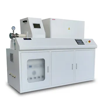
- Chemical Vapor Deposition CVD Equipment System Chamber Slide PECVD Tube Furnace with Liquid Gasifier PECVD Machine
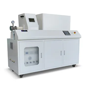
- Inclined Rotary Plasma Enhanced Chemical Vapor Deposition PECVD Equipment Tube Furnace Machine
- Inclined Rotary Plasma Enhanced Chemical Vapor Deposition PECVD Equipment Tube Furnace Machine
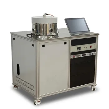
- RF PECVD System Radio Frequency Plasma-Enhanced Chemical Vapor Deposition RF PECVD
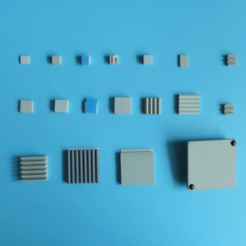
- Silicon Carbide (SIC) Ceramic Sheet Flat Corrugated Heat Sink for Engineering Advanced Fine Ceramics
People Also Ask
- How are carbon nanotubes grown? Master Scalable Production with Chemical Vapor Deposition
- What are the core advantages of PE-CVD in OLED encapsulation? Protect Sensitive Layers with Low-Temp Film Deposition
- What is plasma enhanced chemical vapor deposition PECVD equipment? A Guide to Low-Temperature Thin Film Deposition
- Why is Chemical Vapor Deposition (CVD) equipment uniquely suited for constructing hierarchical superhydrophobic structures?
- What are the advantages of chemical vapor deposition? Achieve Superior Thin Films for Your Lab
