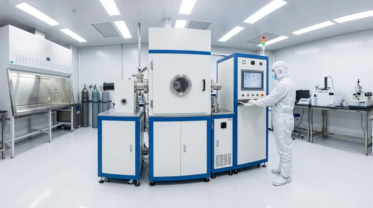
At its core, thin film coating is a process where a solid material is transformed into a vapor, which is then precisely deposited, often atom by atom, onto the surface of a target object, known as a substrate. While multiple methods exist, the most common industrial technique is Physical Vapor Deposition (PVD), which involves vaporizing a source material inside a vacuum and allowing it to condense into a thin, highly durable film.
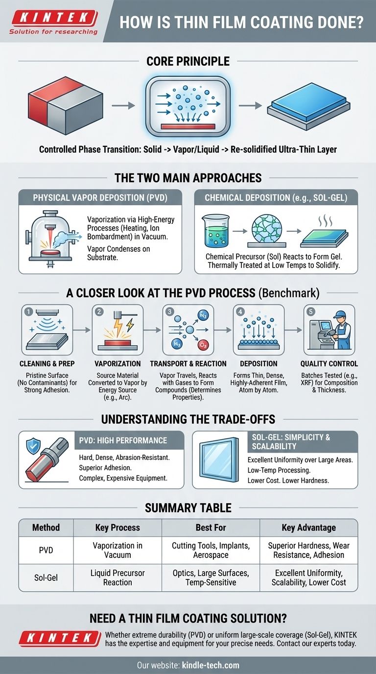
The fundamental principle of thin film coating is not a single method, but a controlled phase transition. It involves taking a solid material, turning it into a vapor or liquid precursor, and then re-solidifying it in a uniform, ultra-thin layer on a substrate's surface.
The Two Main Approaches to Deposition
Thin film coating is a family of processes, not a single technique. Understanding the two primary categories—Physical and Chemical—is key to grasping how different outcomes are achieved.
Physical Vapor Deposition (PVD)
PVD encompasses methods where the coating material is physically transformed into a vapor. This is typically done through high-energy processes like heating or bombardment with ions inside a vacuum chamber. The vaporized material then travels and condenses on the substrate.
Chemical Deposition (e.g., Sol-Gel)
Chemical methods use a chemical precursor, often a liquid solution (the "sol"), that undergoes a series of reactions to form a gel-like network. This precursor is applied to a surface and then thermally treated at low temperatures to create the final solid film.
A Closer Look at the PVD Process
Because of its wide industrial use for creating hard, resistant coatings, the PVD process serves as a benchmark for understanding thin film technology. It generally follows a series of critical steps.
Step 1: Substrate Preparation and Cleaning
The process begins outside the coating chamber. The substrate must be meticulously cleaned to remove any contaminants like oils, dust, or oxides. A pristine surface is non-negotiable for achieving strong adhesion.
Step 2: Vaporization of the Source Material
Inside a high-vacuum chamber, the source material (or "target") is converted into a vapor. This is often achieved by striking it with a high-energy electrical arc, a process also known as ablation. This liberates atoms from the target, creating a metallic vapor.
Step 3: Transport and Reaction
The vaporized atoms travel through the vacuum chamber toward the substrate. During this transport phase, a reactive gas (like nitrogen, oxygen, or a hydrocarbon) can be introduced. The metal atoms react with this gas mid-flight to form new compounds, which will define the film's final properties like color, hardness, and corrosion resistance.
Step 4: Deposition onto the Substrate
The metallic or compound vapor reaches the substrate and condenses on its surface, forming a thin, dense, and highly-adherent film. This happens atom by atom, building a uniform layer that conforms precisely to the part's surface.
Step 5: Post-Process Quality Control
After the coating cycle is complete, batches are tested to ensure consistency. Technicians use tools like an X-ray fluorescent (XRF) machine to verify the coating's elemental composition and thickness, ensuring it meets all required specifications.
Understanding the Trade-offs
Choosing a coating method requires understanding the inherent compromises between different techniques. The "best" process depends entirely on the desired outcome and the constraints of the application.
PVD: High Performance at a Price
PVD creates exceptionally hard, dense, and abrasion-resistant films. The use of a vacuum and high-energy vaporization results in superior adhesion and durability. However, this equipment is complex and expensive, making the process more suitable for high-value or high-performance components.
Sol-Gel: Simplicity and Scalability
The sol-gel method offers significant advantages in simplicity and cost. It does not require a vacuum and operates at much lower temperatures, making it suitable for temperature-sensitive substrates. It also excels at providing excellent film uniformity over very large surface areas. The trade-off is that these films typically do not achieve the same level of hardness or wear resistance as PVD coatings.
Making the Right Choice for Your Application
Your final decision must be guided by the primary goal you need the coating to achieve.
- If your primary focus is maximum durability and wear resistance: PVD is the superior choice for creating hard, long-lasting films for cutting tools, medical implants, or aerospace components.
- If your primary focus is coating a large, temperature-sensitive surface: A chemical method like sol-gel provides excellent uniformity and low-temperature processing, ideal for optics, windows, or certain electronics.
- If your primary focus is achieving a specific color or chemical property: Reactive PVD offers precise control over the film's final composition by introducing specific gases to create nitrides, oxides, or carbides.
Understanding the core principles of vaporization and deposition empowers you to select the technology that best aligns with your project's specific requirements.
Summary Table:
| Method | Key Process | Best For | Key Advantage |
|---|---|---|---|
| PVD (Physical Vapor Deposition) | Vaporization in vacuum chamber | Cutting tools, medical implants, aerospace parts | Superior hardness, wear resistance, and adhesion |
| Sol-Gel (Chemical Deposition) | Liquid precursor reaction at low temperatures | Optics, large surfaces, temperature-sensitive substrates | Excellent uniformity, scalability, and lower cost |
Need a Thin Film Coating Solution Tailored to Your Project?
Whether you require the extreme durability of PVD coatings for high-performance components or the uniform coverage of sol-gel for large-scale applications, KINTEK has the expertise and equipment to meet your laboratory's specific needs. Our range of coating systems ensures precise control over film properties like hardness, color, and chemical resistance.
Contact our experts today to discuss how our thin film coating technologies can enhance your product's performance and longevity.
Visual Guide
Related Products
- Aluminized Ceramic Evaporation Boat for Thin Film Deposition
- Electron Beam Evaporation Coating Oxygen-Free Copper Crucible and Evaporation Boat
- Vacuum Hot Press Furnace Machine for Lamination and Heating
- Molybdenum Tungsten Tantalum Evaporation Boat for High Temperature Applications
- HFCVD Machine System Equipment for Drawing Die Nano-Diamond Coating
People Also Ask
- What are the applications of thin films deposition? Unlock New Possibilities for Your Materials
- What are thin films deposited by evaporation? A Guide to High-Purity Coating
- Why is an alumina boat selected for catalyst precursors? Ensure Sample Purity at 1000 °C
- What are the alternatives to sputtering? Choose the Right Thin Film Deposition Method
- What is thin film deposition? Unlock Advanced Surface Engineering for Your Materials


