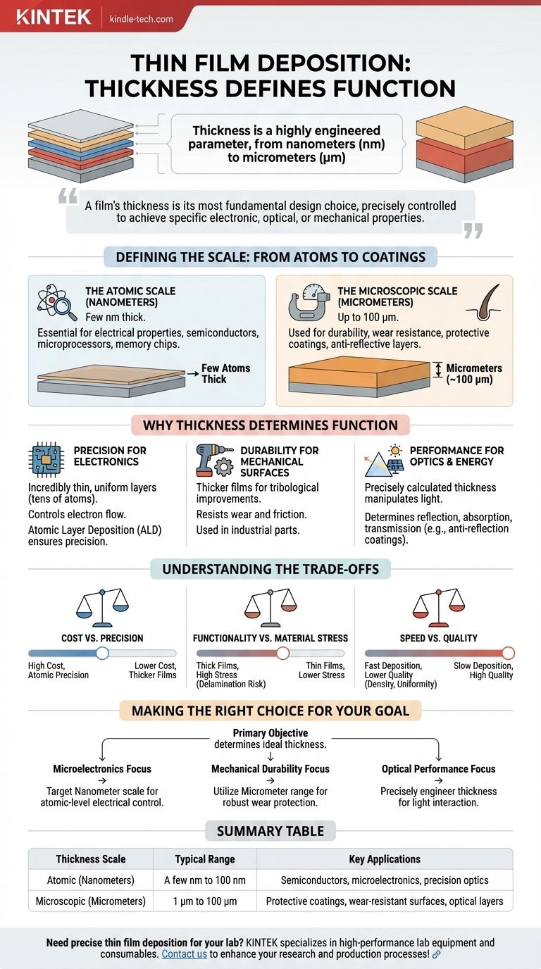
In thin film deposition, thickness is not a single value but a highly engineered parameter. A thin film can range from just a few atoms thick—a few nanometers (nm)—all the way up to 100 micrometers (µm), depending entirely on its intended function.
The critical insight is that a film's thickness is its most fundamental design choice. This dimension is precisely controlled to achieve specific electronic, optical, or mechanical properties, transforming a simple base material into a high-performance component.
Defining the Scale: From Atoms to Coatings
The term "thin film" covers an immense range of scales. Understanding this range is key to grasping why this technology is so versatile and fundamental to modern engineering.
The Atomic Scale (Nanometers)
At the lower end, films are measured in nanometers. A single nanometer is a billionth of a meter.
These ultra-thin layers can be just a few atoms thick. This level of precision is essential in applications where electrical properties are paramount and space is minimal.
This is the world of semiconductors, where films are used to build the foundational components of microprocessors and memory chips.
The Microscopic Scale (Micrometers)
At the upper end, films can reach thicknesses of around 100 micrometers. A micrometer is a millionth of a meter, or about the thickness of a human hair.
These thicker coatings are often used when the primary goal is durability, wear resistance, or creating specific optical effects that require more material.
Applications include protective coatings on cutting tools, anti-reflective layers on lenses, or aesthetic finishes on consumer products.
Why Thickness Determines Function
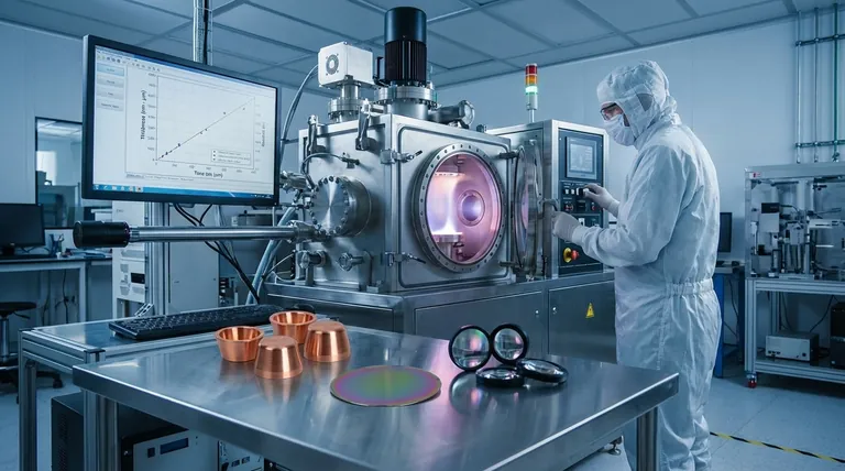
The thickness of a deposited film is not an arbitrary number; it is the primary variable that engineers manipulate to unlock a desired material property. The method of deposition, such as sputtering or atomic layer deposition, is chosen specifically to achieve the required thickness and precision.
Precision for Electronics
In devices like transistors and diodes, films must be incredibly thin and uniform. The flow of electrons is controlled across layers that are often only tens of atoms thick.
Any deviation in thickness can cause the component to fail. This is why processes like Atomic Layer Deposition (ALD), which builds films one atomic layer at a time, are crucial for modern electronics.
Durability for Mechanical Surfaces
For applications requiring tribological improvements—that is, better resistance to wear and friction—thicker films are necessary.
A coating on an industrial drill bit or an automotive engine part needs enough substance to withstand physical abrasion and protect the underlying material. These films are typically in the micrometer range.
Performance for Optics and Energy
In optical devices and solar panels, film thickness is precisely calculated to manipulate light. The thickness determines which wavelengths of light are reflected, absorbed, or transmitted.
For example, an anti-reflection coating on eyeglasses has a thickness carefully tuned to cancel out specific light waves, reducing glare.
Understanding the Trade-offs
Choosing a film thickness involves balancing competing factors. There is no single "best" thickness, only the right thickness for a specific engineering problem.
Cost vs. Precision
Achieving atomic-level precision or depositing very thick films can be time-consuming and therefore more expensive. The deposition process is often a significant factor in the final cost of a component.
Functionality vs. Material Stress
As a film gets thicker, internal stresses can build up. If not properly managed, this stress can cause the film to crack or peel away from the substrate material, a failure known as delamination.
Speed vs. Quality
Faster deposition methods can produce thicker films more quickly but often sacrifice the uniformity and density that are hallmarks of slower, more precise techniques. The choice of method is a critical trade-off between manufacturing speed and final performance.
Making the Right Choice for Your Goal
The ideal film thickness is dictated entirely by your primary objective.
- If your primary focus is microelectronics: Target the nanometer scale to control electrical properties with atomic-level precision.
- If your primary focus is mechanical durability: Utilize thicker films in the micrometer range to provide robust protection against wear and corrosion.
- If your primary focus is optical performance: The thickness must be precisely engineered, often in nanometers, to interact with specific wavelengths of light.
Ultimately, controlling a material's thickness is how you control its function in the modern world.
Summary Table:
| Thickness Scale | Typical Range | Key Applications |
|---|---|---|
| Atomic (Nanometers) | A few nm to 100 nm | Semiconductors, microelectronics, precision optics |
| Microscopic (Micrometers) | 1 µm to 100 µm | Protective coatings, wear-resistant surfaces, optical layers |
Need precise thin film deposition for your lab? KINTEK specializes in high-performance lab equipment and consumables for thin film applications. Whether you're developing next-generation electronics or durable coatings, our solutions ensure the exact thickness control you need. Contact us today to discuss how we can enhance your research and production processes!
Visual Guide
Related Products
- Aluminized Ceramic Evaporation Boat for Thin Film Deposition
- Tungsten Evaporation Boat for Thin Film Deposition
- Electron Beam Evaporation Coating Oxygen-Free Copper Crucible and Evaporation Boat
- Molybdenum Tungsten Tantalum Evaporation Boat for High Temperature Applications
- Vacuum Hot Press Furnace Machine for Lamination and Heating
People Also Ask
- Why is an alumina boat and Ti3AlC2 powder bed necessary for Ti2AlC sintering? Protect MAX Phase Purity
- What is the widely used boat made of in thermal evaporation? Choosing the Right Material for High-Purity Deposition
- Why is an alumina boat selected for catalyst precursors? Ensure Sample Purity at 1000 °C
- Why are high-purity ceramic boats used for lignin activation? Ensure Purity & Thermal Stability
- What are thin films deposited by evaporation? A Guide to High-Purity Coating


