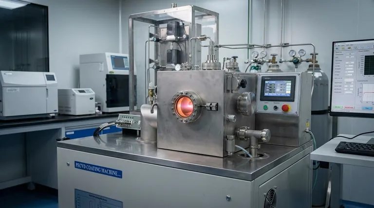
At its core, chemical vapor deposition (CVD) is a process used to create high-purity, high-performance solid thin films from a gas. It involves introducing volatile precursor gases into a reaction chamber, which then decompose and react on a heated substrate surface to form the desired material coating, atom by atom.
Chemical vapor deposition is not a simple coating method; it is a precision manufacturing technique. By carefully controlling gas chemistry, temperature, and pressure, you can build a solid film with a highly specific composition, structure, and thickness directly onto a surface.
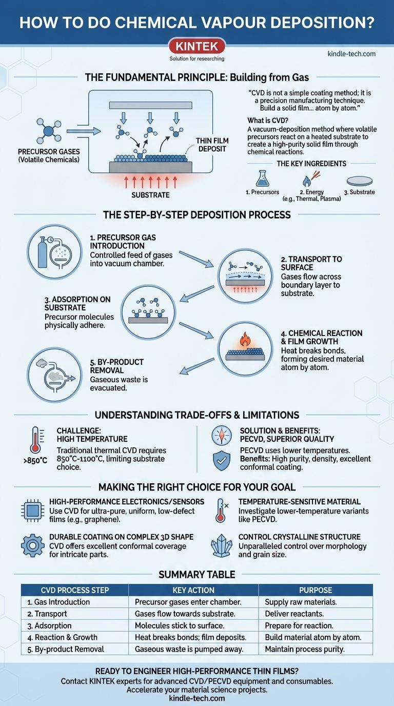
The Fundamental Principle: Building from Gas
What is CVD?
Chemical vapor deposition is a vacuum-deposition method where a substrate is exposed to one or more volatile chemical precursors. These precursors react or decompose on the substrate surface, which is typically heated, to produce the desired thin film deposit.
Unlike physical vapor deposition (PVD), which is like a physical spray of material, CVD is a chemical process. The final film is a new material created by chemical reactions at the moment of deposition.
The Key Ingredients
Every CVD process requires three core components:
- Precursors: Volatile gases or liquids that contain the elements you wish to deposit.
- Energy: Typically high heat (thermal energy) to drive the chemical reactions. Lasers or plasma can also be used.
- Substrate: The material or object onto which the film is grown.
The Step-by-Step Deposition Process
The CVD process is a carefully orchestrated sequence of events happening at a microscopic level.
Step 1: Precursor Gas Introduction
The process begins by feeding precisely controlled amounts of one or more precursor gases into a low-pressure or vacuum reaction chamber.
Step 2: Transport to the Surface
These gases flow toward the heated substrate. As they approach the hot surface, a static gas layer known as the boundary layer forms, which the reactant species must diffuse across to reach the substrate.
Step 3: Adsorption on the Substrate
Once the precursor gas molecules reach the substrate, they physically stick to the surface. This process is called adsorption.
Step 4: The Chemical Reaction and Film Growth
The heat of the substrate provides the energy needed to break chemical bonds in the precursor molecules. This triggers heterogeneous surface reactions, causing the desired solid material to deposit and form a growing film. The molecules may diffuse across the surface to find stable nucleation sites before locking in.
Step 5: By-product Removal
The chemical reactions also create gaseous by-products that are no longer needed. These molecules detach from the surface (desorption), diffuse back across the boundary layer, and are removed from the chamber by the vacuum system's gas flow.
Understanding the Trade-offs and Limitations
No process is perfect. Understanding the trade-offs of CVD is critical for its successful application.
The Primary Challenge: High Temperature
Traditional thermal CVD often requires very high temperatures, typically between 850°C and 1100°C. This high heat can damage or even melt many potential substrate materials, severely limiting its application.
Mitigating the Heat: Lower-Temperature CVD
To overcome this limitation, variants have been developed. Plasma-Enhanced CVD (PECVD) or laser-assisted techniques can drive the necessary chemical reactions at much lower temperatures, making the process compatible with a wider range of substrates.
The Benefit: Superior Film Quality
The main advantage gained from this complexity is exceptional film quality. CVD films are known for their high purity and density.
Furthermore, because the deposition happens from a gas phase, CVD provides excellent conformal coating (or "wrap-around") capabilities, evenly coating complex, non-flat surfaces.
The Power of Control
The true power of CVD lies in its controllability. By adjusting parameters like gas flow rates, temperature, and pressure, you can precisely tailor the film's properties. This includes its chemical composition, crystal structure, grain size, and final thickness. This level of control is what makes CVD a leading method for producing advanced materials like high-quality graphene for electronics and sensors.
Making the Right Choice for Your Goal
To decide if CVD is the right approach, align its capabilities with your primary objective.
- If your primary focus is high-performance electronics or sensors: CVD is a leading choice for creating the ultra-pure, uniform, and low-defect films (like graphene) required for these applications.
- If you need to coat a temperature-sensitive material: Standard thermal CVD is unsuitable, but you should investigate lower-temperature variants like PECVD.
- If you need a durable or functional coating on a complex 3D shape: CVD's excellent conformal coverage makes it a strong candidate for improving hardness, friction, or thermal properties on intricate parts.
- If you need to control the crystalline structure of your film: CVD offers unparalleled control over the morphology and grain size of the deposit, making it ideal for creating specific material phases.
Ultimately, chemical vapor deposition is a powerful tool for engineering materials with precision at the atomic scale.
Summary Table:
| CVD Process Step | Key Action | Purpose |
|---|---|---|
| 1. Gas Introduction | Precursor gases enter the reaction chamber. | Supply the raw materials for the film. |
| 2. Transport | Gases flow towards the heated substrate. | Deliver reactants to the surface. |
| 3. Adsorption | Molecules stick to the substrate surface. | Prepare for the chemical reaction. |
| 4. Reaction & Growth | Heat breaks bonds; solid film deposits. | Build the desired material atom by atom. |
| 5. By-product Removal | Gaseous waste products are pumped away. | Maintain process purity and efficiency. |
Ready to engineer high-performance thin films with precision?
KINTEK specializes in providing the advanced lab equipment and consumables needed for Chemical Vapor Deposition (CVD) and Plasma-Enhanced CVD (PECVD) processes. Whether you are developing next-generation electronics, durable coatings for complex 3D parts, or high-purity materials for research, our expertise and reliable products support your goals for superior film quality, conformal coverage, and precise control.
Contact our experts today to discuss how our solutions can enhance your laboratory's capabilities and accelerate your material science projects.
Visual Guide
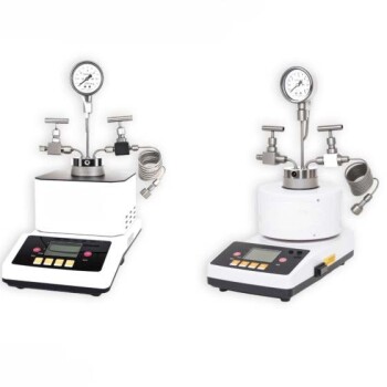
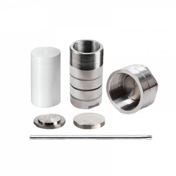
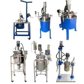
Related Products
- Microwave Plasma Chemical Vapor Deposition MPCVD Machine System Reactor for Lab and Diamond Growth
- 915MHz MPCVD Diamond Machine Microwave Plasma Chemical Vapor Deposition System Reactor
- Customer Made Versatile CVD Tube Furnace Chemical Vapor Deposition Chamber System Equipment
- Cylindrical Resonator MPCVD Machine System Reactor for Microwave Plasma Chemical Vapor Deposition and Lab Diamond Growth
- Split Chamber CVD Tube Furnace with Vacuum Station Chemical Vapor Deposition System Equipment Machine
People Also Ask
- What pressure is needed for chemical vapor deposition of diamonds? Master the Low-Pressure 'Sweet Spot'
- How does a microwave plasma reactor facilitate the synthesis of diamond? Master MPCVD with Precision Technology
- How does MPCVD work? A Guide to Low-Temperature, High-Quality Film Deposition
- What are the primary advantages of the CVD method for growing diamonds? Engineering High-Purity Gems and Components
- What is microwave plasma chemical vapor deposition? A Guide to High-Purity Diamond Film Growth