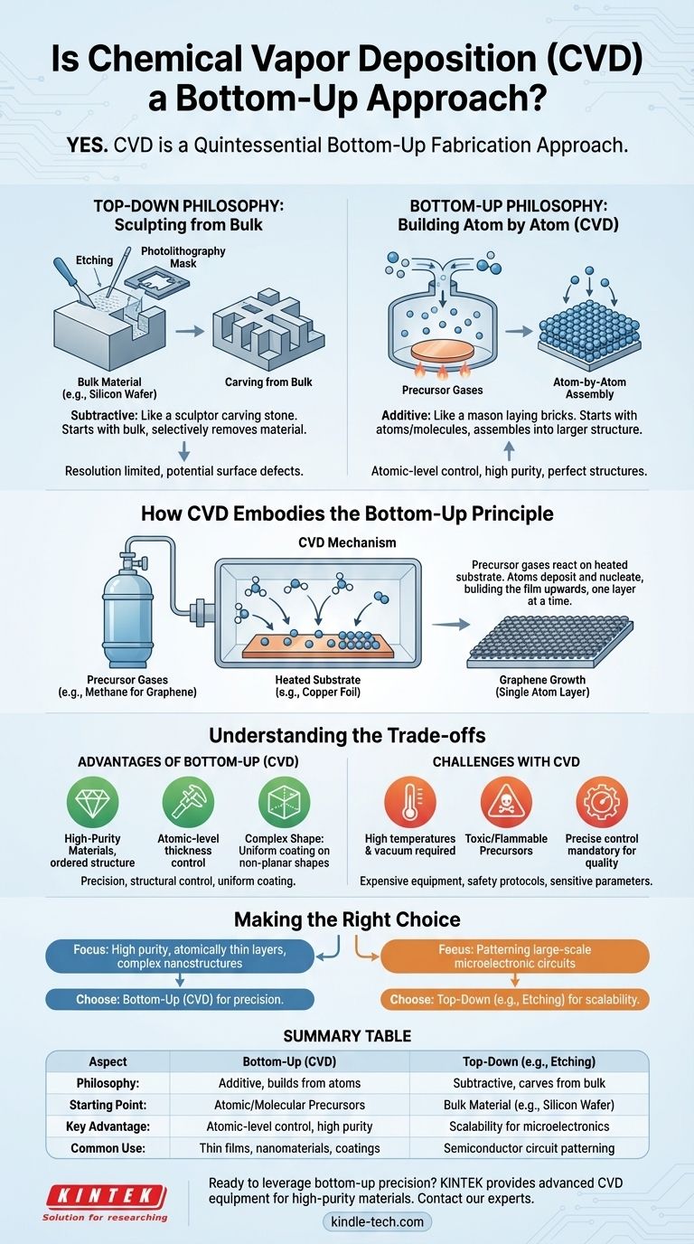
Yes, Chemical Vapor Deposition (CVD) is a quintessential bottom-up fabrication approach. Unlike methods that carve material away from a larger block, CVD constructs materials from the ground up by assembling them atom by atom or molecule by molecule. This additive process allows for exceptional control over the material's thickness, purity, and structure on a nanoscale level.
The core distinction lies in the manufacturing philosophy. "Top-down" methods are subtractive, like a sculptor carving stone, while "bottom-up" methods like CVD are additive, like a mason precisely laying one brick at a time to build a wall.
What Defines "Bottom-Up" vs. "Top-Down"
To understand why CVD fits its category, it's essential to grasp the two fundamental approaches to micro and nano-fabrication.
The "Top-Down" Philosophy: Sculpting from Bulk
Top-down manufacturing starts with a large piece of bulk material, often a silicon wafer.
Techniques like photolithography and etching are then used to selectively remove material, carving out the desired pattern or structure.
This approach is dominant in traditional microelectronics manufacturing but can be limited by the resolution of the tools and can introduce surface defects during the removal process.
The "Bottom-Up" Philosophy: Building Atom by Atom
Bottom-up manufacturing is the reverse. It begins with atomic or molecular precursors and systematically assembles them into a larger, more complex structure.
This method offers the potential for creating materials with near-atomic precision and perfect structures because you are defining the material as you build it.
Techniques in this category include CVD, Atomic Layer Deposition (ALD), and molecular self-assembly.
How CVD Embodies the Bottom-Up Principle
The very mechanism of Chemical Vapor Deposition is a clear demonstration of the bottom-up approach in action.
The Core Mechanism: Precursors to Solid Film
The process begins by introducing precursor gases into a reaction chamber containing a substrate (the surface to be coated).
When these gases reach the heated substrate, they undergo a chemical reaction or decomposition. This reaction causes the desired atoms to "deposit" onto the substrate surface.
Building Layer by Layer
These atoms nucleate and grow, forming a continuous thin film. The film is literally built from the substrate upwards, one atomic layer at a time.
This additive nature is the essence of bottom-up fabrication. By precisely controlling process parameters like temperature, pressure, and gas flow, engineers can dictate the film's thickness and composition with incredible accuracy.
An Example in Action: Graphene Growth
A classic example is the growth of a single-atom-thick sheet of graphene. Methane gas (a carbon precursor) is flowed over a heated copper foil substrate.
The methane decomposes, and carbon atoms arrange themselves on the copper surface into the hexagonal lattice of graphene, demonstrating a perfect build-up from atomic components.
Understanding the Trade-offs
Choosing a fabrication method requires understanding its inherent advantages and challenges. The bottom-up nature of CVD presents a distinct set of trade-offs.
Advantages of the Bottom-Up Approach
CVD allows for the creation of exceptionally high-purity materials and highly ordered crystal structures, as there are no defects introduced from a carving process.
It provides atomic-level control over thickness, which is critical for modern semiconductor devices and optical coatings.
The technique is also excellent for coating complex, non-planar shapes uniformly, as the precursor gas can reach all surfaces.
Potential Challenges with CVD
CVD processes often require high temperatures and vacuum conditions, necessitating specialized and expensive equipment.
The precursor chemicals used can be highly toxic, flammable, or corrosive, requiring stringent safety protocols.
The final quality of the film is extremely sensitive to process parameters, meaning precise control is mandatory to achieve consistent and repeatable results.
Making the Right Choice for Your Application
The decision between a bottom-up or top-down method depends entirely on the intended outcome.
- If your primary focus is creating high-purity, atomically thin layers or complex nanostructures: A bottom-up method like CVD is the superior choice for its precision and structural control.
- If your primary focus is patterning large-scale microelectronic circuits from a silicon wafer: A top-down method like photolithography and etching remains the industry standard for its established scalability and efficiency.
Understanding this fundamental distinction between building up and carving down is the first step toward mastering nanoscale fabrication.
Summary Table:
| Aspect | Bottom-Up (CVD) | Top-Down (e.g., Etching) |
|---|---|---|
| Philosophy | Additive: Builds from atoms/molecules | Subtractive: Carves from bulk material |
| Starting Point | Atomic/Molecular Precursors | Bulk Material (e.g., Silicon Wafer) |
| Key Advantage | Atomic-level control, high-purity films | Scalability for microelectronics |
| Common Use | Thin films, nanomaterials, coatings | Semiconductor circuit patterning |
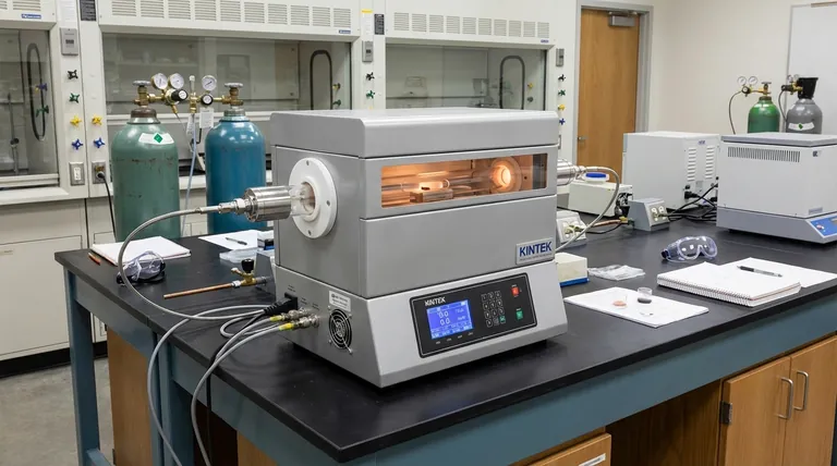
Ready to leverage the precision of bottom-up fabrication in your lab? KINTEK specializes in providing the advanced CVD equipment and consumables you need to create high-purity, atomically precise materials. Our expertise ensures you achieve consistent, high-quality results for your most demanding applications. Contact our experts today to discuss how our solutions can enhance your research and development!
Visual Guide
Related Products
- Chemical Vapor Deposition CVD Equipment System Chamber Slide PECVD Tube Furnace with Liquid Gasifier PECVD Machine
- RF PECVD System Radio Frequency Plasma-Enhanced Chemical Vapor Deposition RF PECVD
- Microwave Plasma Chemical Vapor Deposition MPCVD Machine System Reactor for Lab and Diamond Growth
- Customer Made Versatile CVD Tube Furnace Chemical Vapor Deposition Chamber System Equipment
- 915MHz MPCVD Diamond Machine Microwave Plasma Chemical Vapor Deposition System Reactor
People Also Ask
- How are carbon nanotubes grown? Master Scalable Production with Chemical Vapor Deposition
- What are the advantages of chemical vapor deposition? Achieve Superior Thin Films for Your Lab
- What are the processes of vapor phase deposition? Understand CVD vs. PVD for Superior Thin Films
- What types of substrates are used in CVD to facilitate graphene films? Optimize Graphene Growth with the Right Catalyst
- What are the core advantages of PE-CVD in OLED encapsulation? Protect Sensitive Layers with Low-Temp Film Deposition


