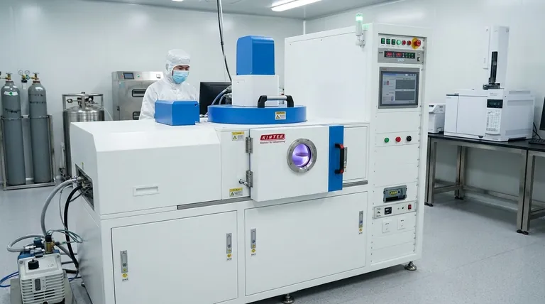
In semiconductor manufacturing, a sputtering target is a high-purity source material used to deposit microscopic thin films onto a silicon wafer. This process, known as sputtering, involves bombarding the target with energized ions, which dislodges atoms from the target that then travel and coat the wafer. These ultra-thin layers form the essential conductive, insulating, and protective structures of an integrated circuit.
The key is to see a sputtering target not as a simple piece of raw material, but as a highly engineered component. Its extreme purity and precise physical characteristics directly determine the performance, quality, and reliability of the final microchip.
The Role of Sputtering in Chip Fabrication
At its core, manufacturing a semiconductor is a process of building a complex, three-dimensional structure one atomic layer at a time. Sputtering is one of the primary methods for depositing these precise layers.
The Sputtering Process Explained
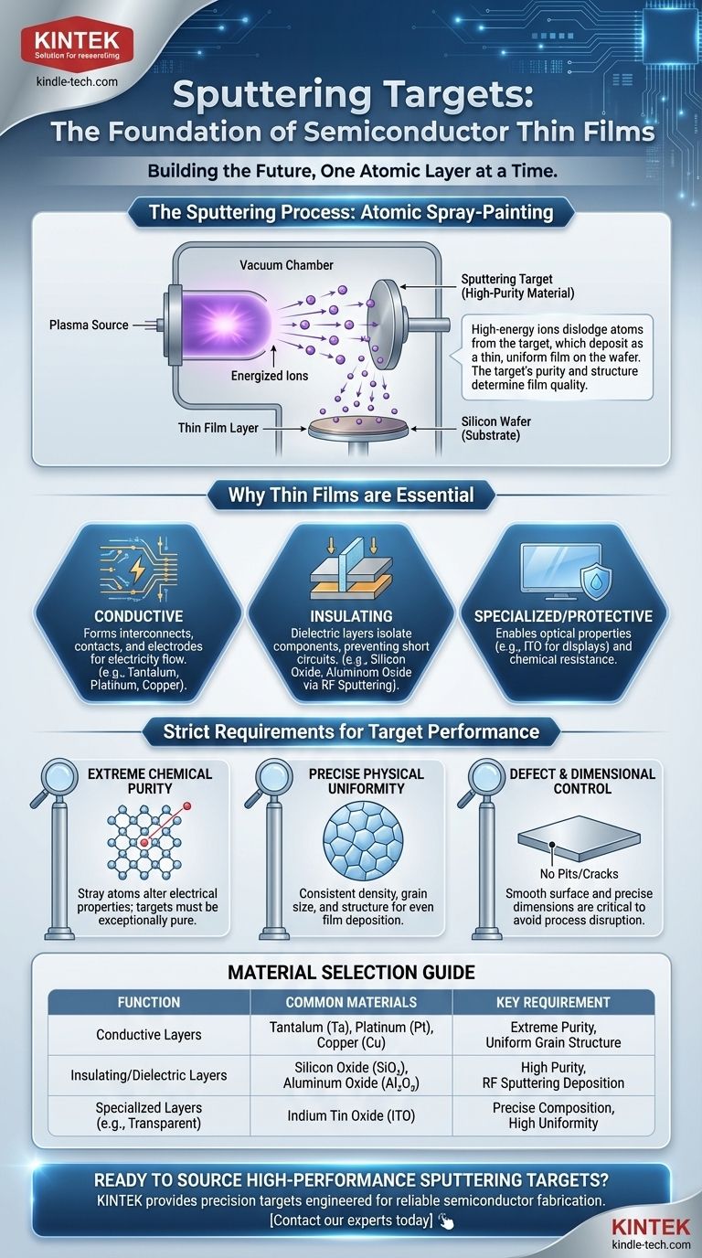
Think of sputtering as a form of "atomic spray-painting." A high-purity disc or plate of the desired material—the sputtering target—is placed in a vacuum chamber. High-energy ions, typically from an inert gas like argon, are fired at the target. This impact knocks individual atoms or molecules off the target's surface, which then travel and deposit as a thin, uniform film on the semiconductor wafer.
Why Thin Films are Essential
These deposited layers are the functional building blocks of a microchip. A single chip may have dozens or even hundreds of these films, each with a specific purpose.
The films can be conductive (forming the microscopic wiring), insulating or dielectric (preventing short circuits between wires), or protective (providing chemical resistance to protect the delicate circuitry).
The Target as the Source of Quality
The quality of the deposited film can only be as good as the source material. Any impurity or structural defect in the sputtering target will be transferred directly to the film on the wafer, potentially creating a faulty microchip. This is why the requirements for targets are so stringent.
Common Target Materials and Their Functions
Different materials are chosen for sputtering targets based on the specific electrical or physical properties required for each layer of the integrated circuit.
Conductive Metal Layers
Targets made of materials like Tantalum (Ta) or Platinum (Pt) are used to create the microscopic interconnects, contacts, and electrodes that allow electricity to flow through the circuit.
Insulating Dielectric Layers
To isolate these conductive pathways from one another, insulating films are required. RF Sputtering is a specific technique used with targets like Silicon Oxide (SiO₂) or Aluminum Oxide (Al₂O₃) to deposit these non-conductive, dielectric layers.
Specialized Optical and Electronic Layers
Sputtering is also used for more specialized applications. For example, Indium Tin Oxide (ITO) targets are used to create films that are both transparent and conductive, essential for flat-panel displays and solar cells.
The Strict Requirements for Sputtering Targets
The performance demands of modern electronics mean that sputtering targets must meet standards far beyond those of traditional materials. Any deviation can lead to device failure.
Extreme Chemical Purity
Even a few stray atoms of an unwanted element per million can alter the electrical properties of the semiconductor, rendering the entire device useless. Targets must therefore be refined to exceptional levels of purity.
Precise Physical Uniformity
The density, grain size, and crystalline structure of the target must be perfectly uniform. Any variation across the target's surface will cause the film to deposit unevenly on the wafer, leading to defects.
Defect and Dimensional Control
The target itself must be manufactured to precise dimensions with a perfectly flat and smooth surface. Any pits, cracks, or warping in the target will disrupt the sputtering process and compromise the quality of the deposited layer.
Making the Right Choice for Your Goal
The selection of a sputtering target is dictated entirely by the function of the layer being created.
- If your primary focus is creating conductive pathways: You will utilize metal targets like Tantalum, Platinum, or Copper to form the circuit's wiring and contacts.
- If your primary focus is isolating components: You will need dielectric targets, such as Silicon Oxide or Tantalum Oxide, often deposited using RF sputtering.
- If your primary focus is building specialized devices: You will turn to application-specific targets like Indium Tin Oxide for displays or exotic alloys for memory chips and sensors.
Ultimately, the sputtering target is the foundational source from which the intricate, high-performance layers of modern electronic devices are built.
Summary Table:
| Function | Common Target Materials | Key Requirement |
|---|---|---|
| Conductive Layers (Wiring, Contacts) | Tantalum (Ta), Platinum (Pt), Copper (Cu) | Extreme Purity, Uniform Grain Structure |
| Insulating/Dielectric Layers | Silicon Oxide (SiO₂), Aluminum Oxide (Al₂O₃) | High Purity, Deposited via RF Sputtering |
| Specialized Layers (e.g., Transparent Conductive) | Indium Tin Oxide (ITO) | Precise Composition, High Uniformity |
Ready to source high-performance sputtering targets for your semiconductor fabrication?
KINTEK specializes in providing high-purity lab equipment and consumables, including precision sputtering targets for conductive, dielectric, and specialized thin film applications. Our materials are engineered to meet the stringent purity and uniformity requirements essential for reliable microchip production.
Contact our experts today to discuss your specific needs and ensure the quality of your semiconductor layers from the source.
Visual Guide
Related Products
- Custom PTFE Wafer Holders for Lab and Semiconductor Processing
- Customizable PTFE Wafer Carriers for Semiconductor and Lab Applications
People Also Ask
- Why is a custom PTFE sample holder necessary for CBD of Cd(1-x)ZnxS thin films? Ensure High Purity and Uniformity
- Why is a PTFE container required for acid leaching of silicon nanosheets? Ensure High Purity and Safety
- How do PTFE holders or laboratory presses contribute to electrode prep? Ensure Precision in Corrosion Testing
- How does a custom PTFE electrode holder contribute to the accuracy of immersion tests? Ensure Precise Steel Analysis
- Why use high-quality PTFE containers for CO2 reduction electrolytes? Eliminate silicon contamination and ensure data.