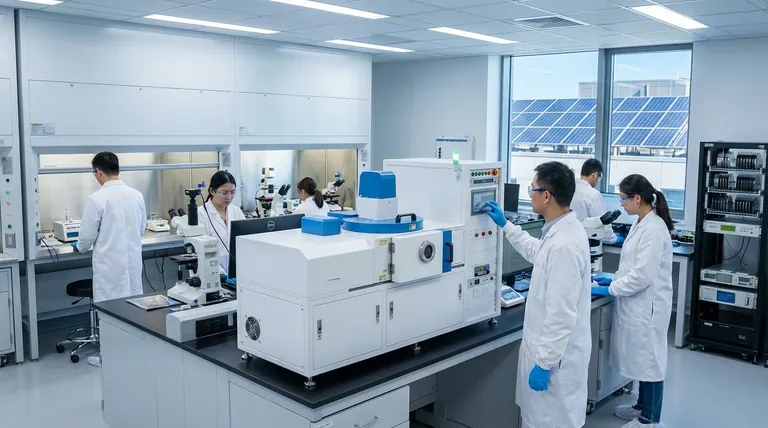
In short, thin film technology is foundational to virtually all modern technology. Its applications range from the microchips in your smartphone and the screen you are reading this on, to advanced solar panels, durable industrial coatings, and life-saving biomedical implants. This technology involves depositing microscopic layers of material onto a surface to grant it new, specific properties.
The core value of thin film technology is not in creating a single product, but in its ability to precisely modify a material's surface. By adding ultra-thin, functional layers, we can make an object conductive, reflective, corrosion-resistant, or able to convert light into energy.
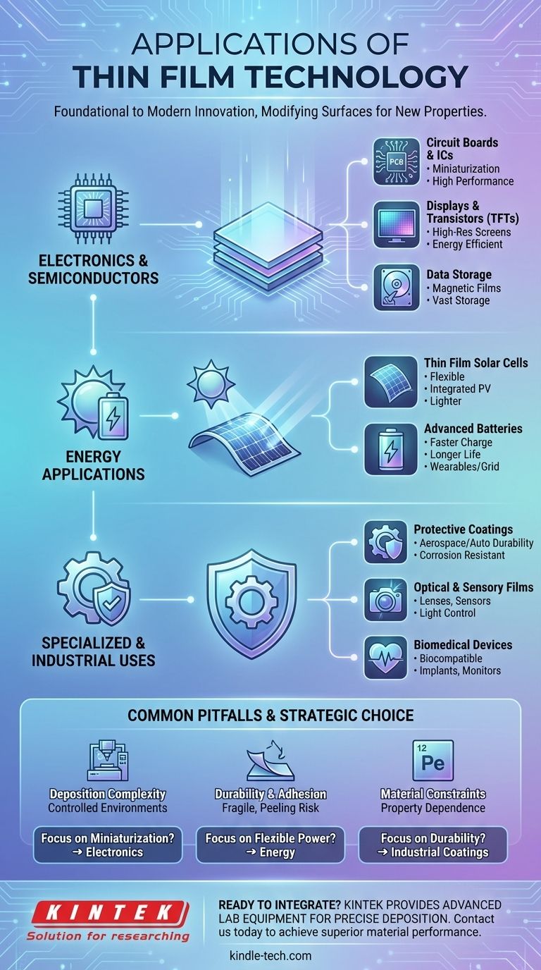
The Foundation: Electronics and Semiconductors
Thin film deposition is the engine of the digital revolution. Its ability to create microscopic, layered structures is essential for manufacturing the high-performance electronic components that power our world.
Circuit Boards and Integrated Circuits
Thin films are used to produce the intricate conductive pathways on printed circuit boards (PCBs) and integrated circuits (ICs). This allows for extreme miniaturization, packing immense processing power into small devices.
This technology is also critical for microelectromechanical systems (MEMS), which combine tiny mechanical devices and electronics on a single chip.
Displays and Transistors
Nearly every modern flat-panel display relies on thin film transistors (TFTs). These microscopic switches control individual pixels in LCD and OLED screens.
The use of thin films in displays enables higher resolutions, better energy efficiency, and faster response times, which are crucial for everything from TVs to smartwatches.
Data Storage
The surfaces of hard disk drives are coated with thin magnetic films. These layers are engineered to store vast amounts of data by magnetizing microscopic regions, forming the basis of modern digital storage.
Powering the Future: Energy Applications
Thin film technology is playing a pivotal role in developing next-generation energy solutions that are more efficient, flexible, and integrated into our environment.
Thin Film Solar Cells
Unlike traditional rigid silicon panels, thin film solar cells are created by depositing photovoltaic material onto a substrate. This makes them significantly lighter and more flexible.
This flexibility allows them to be used in innovative applications like photovoltaic glazing (solar-capturing windows) and integrated into the body of vehicles or portable devices.
Advanced Batteries
Thin film batteries are a major leap forward in energy storage. They are smaller, charge much faster, last longer, and are more efficient than their conventional counterparts.
Their compact size and high performance make them ideal for medical implants, smart cards, wearable technology, and grid-scale green energy storage banks.
Beyond Electronics: Specialized and Industrial Uses
The ability to engineer a surface's properties has led to widespread adoption in demanding industrial, optical, and biomedical fields.
Protective and Mechanical Coatings
Thin film deposition can create super-hard, corrosion-resistant, and heat-resistant coatings. These films protect critical components in the aerospace, automotive, and manufacturing industries.
Tools, engine parts, and military equipment are often coated to extend their lifespan and improve performance under extreme conditions.
Optical and Sensory Films
Thin films are used to create highly specialized optical coatings on lenses for cameras and scientific instruments, controlling reflection and transmission of light.
They are also used to create a wide variety of sensors, including films that are sensitive to light, heat, or specific chemicals for use in scientific and medical devices.
Biomedical Devices
In biomedicine, thin films are essential for creating devices like hearing aids and wearable health monitors. The technology enables the creation of biocompatible coatings for medical implants, ensuring they are not rejected by the body.
Common Pitfalls to Avoid
While powerful, thin film technology is not a universal solution. Understanding its limitations is key to successful application.
Deposition Complexity
Applying a perfect, uniform thin film requires highly controlled environments and expensive, specialized equipment. The process itself can be slow and complex.
Durability and Adhesion
By their nature, thin films can be fragile. Ensuring the film adheres properly to the substrate material without peeling or cracking is a major engineering challenge, especially for flexible applications or harsh environments.
Material Constraints
The final performance of the component is entirely dependent on the properties of the material being deposited. Finding a material that is durable, stable, and possesses the desired electrical, optical, or mechanical properties can be difficult.
Making the Right Choice for Your Goal
The right application of thin film technology depends entirely on the problem you need to solve.
- If your primary focus is miniaturization and efficiency in electronics: Thin film deposition is the non-negotiable standard for creating compact, high-performance integrated circuits and displays.
- If your primary focus is flexible or integrated renewable energy: Thin film solar cells and batteries provide lightweight and versatile power solutions that traditional technologies cannot match.
- If your primary focus is material durability and performance: Specialized thin film coatings are the most effective way to protect critical components from wear, heat, and corrosion.
Ultimately, thin film technology is a fundamental enabler, transforming simple materials into high-performance components that define modern innovation.
Summary Table:
| Application Area | Key Examples | Core Benefit |
|---|---|---|
| Electronics & Semiconductors | Circuit Boards, Displays (TFTs), Data Storage | Enables miniaturization and high performance |
| Energy | Thin Film Solar Cells, Advanced Batteries | Provides flexible, efficient power solutions |
| Industrial & Specialized | Protective Coatings, Optical Films, Biomedical Devices | Enhances durability, functionality, and biocompatibility |
Ready to integrate thin film technology into your project?
KINTEK specializes in providing the advanced lab equipment and consumables essential for precise thin film deposition. Whether you are developing next-generation electronics, efficient solar panels, or durable industrial coatings, our solutions support your innovation from R&D to production.
Contact us today using the form below to discuss how we can help you achieve superior material performance and bring your ideas to life.
Visual Guide
Related Products
- Aluminized Ceramic Evaporation Boat for Thin Film Deposition
- Electron Beam Evaporation Coating Oxygen-Free Copper Crucible and Evaporation Boat
- Vacuum Hot Press Furnace Machine for Lamination and Heating
- Molybdenum Tungsten Tantalum Evaporation Boat for High Temperature Applications
- HFCVD Machine System Equipment for Drawing Die Nano-Diamond Coating
People Also Ask
- Why is an alumina boat selected for catalyst precursors? Ensure Sample Purity at 1000 °C
- What is the chemical method for thin film deposition? Build Films from the Molecular Level Up
- What is the widely used boat made of in thermal evaporation? Choosing the Right Material for High-Purity Deposition
- What are the applications of thin films deposition? Unlock New Possibilities for Your Materials
- Why are high-purity ceramic boats used for lignin activation? Ensure Purity & Thermal Stability


