In short, vacuum deposition is a foundational manufacturing process used to apply extremely thin, high-performance films onto a surface. These applications span a vast range of industries, from creating anti-reflective coatings on eyeglasses and conductive layers in solar cells to applying durable, decorative finishes on consumer products and protective barriers on food packaging.
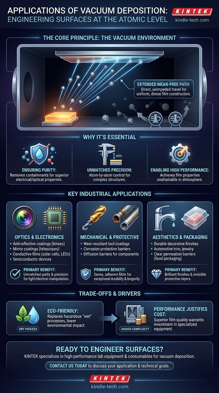
The core principle is not the material being deposited, but the environment in which it is done. By removing virtually all air and contaminants, a vacuum allows for the atom-by-atom or molecule-by-molecule construction of a film, granting a level of purity, precision, and performance that is unattainable in a normal atmosphere.
Why a Vacuum is Essential for High-Performance Coatings
The term "vacuum deposition" refers to a family of processes, but they are all unified by the need for a low-pressure environment. Understanding why this is necessary is key to understanding its wide-ranging applications.
Ensuring Purity and Preventing Contamination
In a normal atmosphere, a surface is constantly bombarded by particles like oxygen, nitrogen, and water vapor. Attempting to deposit a thin film in these conditions would be like trying to paint a wall during a dust storm.
The vacuum chamber removes these contaminants, preventing them from being trapped in the film. This is critical for applications where purity dictates performance, as even trace amounts of oxygen can ruin the electrical or optical properties of a coating.
Enabling a Direct Path to the Surface
At atmospheric pressure, vaporized atoms can only travel a microscopic distance before colliding with an air molecule. This is known as a short "mean-free path."
Creating a vacuum extends this path, allowing atoms from the source material to travel in a straight line directly to the target surface. This ensures a uniform, dense, and adherent film rather than a porous, soot-like deposit.
Achieving Unmatched Precision and Control
Because deposition occurs in a sterile, controlled environment, the process offers unparalleled precision. Engineers can control film thickness down to the nanometer range, building up layers atom-by-atom.
This level of control is what enables the creation of complex structures like optical interference filters or advanced semiconductor devices.
A Survey of Key Industrial Applications
The control offered by the vacuum environment makes the process uniquely suited for solving problems across different industries.
Optics and Electronics
Purity and precision are paramount in these fields. Vacuum deposition is used to create anti-reflective coatings on lenses, mirror coatings on telescopes, and electrically conductive films for LED displays and solar cells. It is also the backbone of manufacturing semiconductor devices and integrated circuits.
Mechanical and Protective Functions
For these applications, density and adhesion are key. The process is used to apply exceptionally hard, wear-resistant coatings to cutting tools and machine parts, significantly extending their operational life. It also creates dense corrosion-protective coatings and diffusion barriers that shield sensitive components from the environment.
Aesthetics and Packaging
Vacuum deposition can produce brilliant, durable decorative coatings on everything from automotive trim to faucets and jewelry. In the packaging industry, it is used to apply an invisibly thin metallic or ceramic layer onto polymer films, creating a clear permeation barrier that keeps food fresh without affecting transparency.
Understanding the Trade-offs and Drivers
While powerful, vacuum deposition is chosen for specific reasons, often involving important trade-offs.
The Environmental Advantage
Many traditional coating methods, like electroplating with chromium or cadmium, are "wet" processes that involve hazardous chemicals and produce toxic waste.
Vacuum deposition is a "dry process" with a significantly lower environmental impact. This ecological cleanliness is a major driver for its adoption as a replacement for older, more hazardous techniques.
Process Complexity and Cost
Achieving and maintaining a high vacuum requires specialized and expensive equipment, including chambers, high-power pumps, and sophisticated monitoring systems.
The process is more complex and has a higher capital cost than simpler methods like painting. However, the superior performance, purity, and durability of the resulting films often justify the investment for high-value applications.
Versatility vs. Specialization
While the family of vacuum deposition techniques is highly versatile, an individual system is often configured for a specific material and application. Optimizing a machine for depositing a metallic alloy for wear resistance is very different from optimizing one for a multi-layer optical filter.
How to Apply This to Your Technical Goals
Your choice to use vacuum deposition should be driven by the specific performance you require from a surface.
- If your primary focus is performance and purity: The key takeaway is that the clean vacuum environment is non-negotiable for creating films whose optical or electrical properties would be destroyed by contamination.
- If your primary focus is surface protection: The key is creating a dense, non-porous barrier to resist wear or corrosion, a structure that is physically impossible to form in a normal atmosphere where atoms would scatter.
- If your primary focus is replacing a hazardous process: The key takeaway is that vacuum deposition offers a 'dry,' environmentally cleaner alternative for achieving similar or superior functional coatings.
Ultimately, vacuum deposition is the definitive tool for engineering surfaces at the atomic level, enabling performance impossible to achieve by other means.
Summary Table:
| Application Category | Key Examples | Primary Benefit |
|---|---|---|
| Optics & Electronics | Anti-reflective lenses, solar cells, semiconductors | Unmatched purity and precision for electrical/optical properties |
| Mechanical & Protective | Wear-resistant tool coatings, corrosion barriers | Dense, adherent films for durability and longevity |
| Aesthetics & Packaging | Decorative finishes, food packaging barriers | Brilliant, durable finishes and clear permeation barriers |
Ready to engineer surfaces at the atomic level?
KINTEK specializes in high-performance lab equipment and consumables for vacuum deposition processes. Whether you're developing advanced semiconductors, durable protective coatings, or innovative packaging solutions, our expertise ensures you achieve the purity, precision, and performance your projects demand.
Contact us today to discuss how our solutions can enhance your coating applications and meet your technical goals!
Visual Guide
Related Products
- Chemical Vapor Deposition CVD Equipment System Chamber Slide PECVD Tube Furnace with Liquid Gasifier PECVD Machine
- Molybdenum Tungsten Tantalum Evaporation Boat for High Temperature Applications
- Inclined Rotary Plasma Enhanced Chemical Vapor Deposition PECVD Equipment Tube Furnace Machine
- Inclined Rotary Plasma Enhanced Chemical Vapor Deposition PECVD Equipment Tube Furnace Machine
- HFCVD Machine System Equipment for Drawing Die Nano-Diamond Coating
People Also Ask
- What are the core advantages of PE-CVD in OLED encapsulation? Protect Sensitive Layers with Low-Temp Film Deposition
- Why is Chemical Vapor Deposition (CVD) equipment uniquely suited for constructing hierarchical superhydrophobic structures?
- What are the advantages of chemical vapor deposition? Achieve Superior Thin Films for Your Lab
- What is the chemical vapor deposition growth process? Build Superior Thin Films from the Atom Up
- What are the processes of vapor phase deposition? Understand CVD vs. PVD for Superior Thin Films