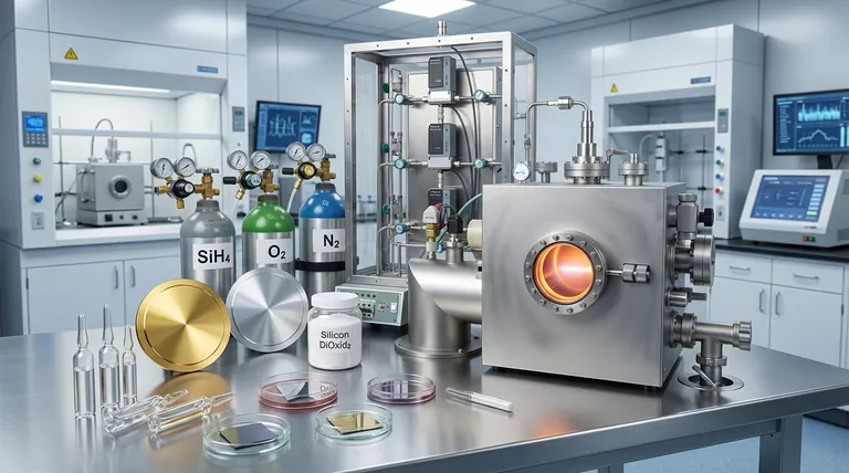
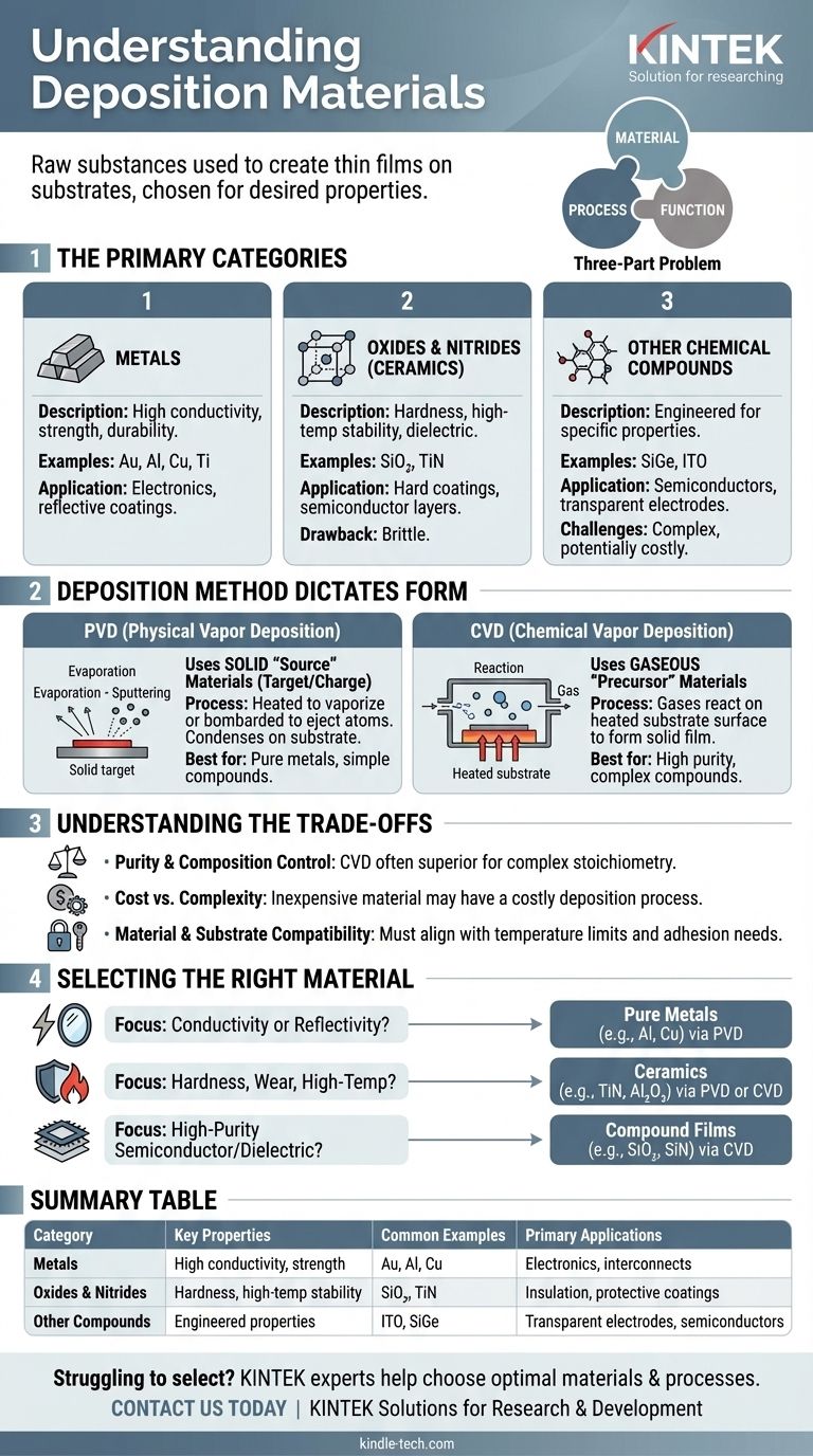
In essence, deposition materials are the raw substances used to create a thin film on a surface, known as a substrate. The most common categories are pure metals (like gold or aluminum), oxides and nitrides (ceramics like silicon dioxide), and more complex chemical compounds. The choice of material is dictated by the desired properties of the final film, such as its strength, conductivity, or resistance to heat.
The selection of a deposition material is not an isolated decision. It is fundamentally linked to both the deposition method you use and the specific performance characteristics required for the final application, creating a three-part problem of material, process, and function.
The Primary Categories of Deposition Materials
Deposition materials are generally grouped by their chemical nature. Each category offers a distinct profile of properties, benefits, and challenges.
Metals
Metals are chosen for their excellent electrical and thermal conductivity, strength, and durability. They are foundational in electronics and for creating reflective or protective coatings.
Common examples include aluminum (Al), copper (Cu), gold (Au), and titanium (Ti). While effective, purer metals can be expensive, influencing their use in high-value applications.
Oxides and Nitrides (Ceramics)
This category, which includes materials like silicon dioxide (SiO₂) and titanium nitride (TiN), is known for durability, hardness, and the ability to withstand very high temperatures.
They are often used as dielectric layers in semiconductors, hard coatings on cutting tools, or as thermal barriers. Their primary drawback is that they tend to be brittle.
Other Chemical Compounds
This is a broad category encompassing any material formed from two or more elements, such as semiconductors or specialized alloys. Examples include silicon germanium (SiGe) or transparent conducting oxides like indium tin oxide (ITO).
These compounds can be engineered for very specific optical, electrical, or mechanical properties. However, their complexity can make them difficult to work with and potentially more expensive to deposit.
How Deposition Method Dictates Material Form
The physical form of the starting material is determined by the deposition technology being used. The two main approaches, Physical Vapor Deposition (PVD) and Chemical Vapor Deposition (CVD), handle materials very differently.
PVD and Solid "Source" Materials
Physical Vapor Deposition (PVD) methods, such as thermal evaporation or sputtering, begin with a solid source material (often called a target or charge).
This solid is heated in a high vacuum until it vaporizes (evaporation) or is bombarded with ions to eject atoms (sputtering). The resulting vapor stream then travels and condenses on the substrate, forming the thin film. This method is straightforward for depositing pure metals and some simple compounds.
CVD and Gaseous "Precursor" Materials
Chemical Vapor Deposition (CVD) does not use a solid source in the same way. Instead, it introduces one or more precursor gases into a reaction chamber.
These "reacting gaseous species" are catalyzed by the heated substrate surface, causing them to react and decompose to form the desired solid film. This process is ideal for creating highly pure and complex compound films, such as silicon dioxide or silicon nitride, that would be difficult or impossible to create with PVD.
Understanding the Trade-offs
Choosing a material involves balancing performance, cost, and process limitations. A material that is perfect in theory may be impractical to implement.
Purity and Composition Control
Maintaining the exact chemical composition (stoichiometry) of the source material in the final film can be a significant challenge, especially for complex compounds in PVD processes. CVD often offers superior control over film purity and composition because the flow of precursor gases can be precisely metered.
Cost vs. Process Complexity
A material itself may be inexpensive, but the process required to deposit it can be costly. While some metals are expensive raw materials, complex compounds may require difficult and expensive precursor gases for a CVD process, driving up the total cost.
Material and Substrate Compatibility
The chosen material and its deposition process must be compatible with the substrate. A high-temperature CVD process, for example, cannot be used to coat a low-melting-point plastic substrate. The adhesion of the film material to the substrate is also a critical consideration.
Selecting the Right Material for Your Application
Your end goal is the most important factor in material selection. Base your decision on the primary function the thin film must serve.
- If your primary focus is electrical conductivity or reflectivity: Prioritize pure metals like aluminum, copper, silver, or gold, likely deposited via a PVD method.
- If your primary focus is hardness, wear resistance, or high-temperature stability: Look to ceramics like oxides (e.g., Al₂O₃) and nitrides (e.g., TiN), which can be deposited by either PVD or CVD.
- If your primary focus is creating a high-purity semiconductor or dielectric layer: You will almost certainly need a CVD process using specific precursor gases to form precise compound films like silicon, silicon dioxide, or silicon nitride.
Ultimately, the right deposition material is the one whose properties and process compatibility best align with the performance goals of your final product.
Summary Table:
| Category | Key Properties | Common Examples | Primary Applications |
|---|---|---|---|
| Metals | High electrical/thermal conductivity, strength, durability | Gold (Au), Aluminum (Al), Copper (Cu) | Electronics, reflective coatings, interconnects |
| Oxides & Nitrides | Hardness, high-temperature stability, dielectric properties | Silicon Dioxide (SiO₂), Titanium Nitride (TiN) | Semiconductor insulation, hard protective coatings |
| Other Compounds | Engineered optical, electrical, or mechanical properties | Indium Tin Oxide (ITO), Silicon Germanium (SiGe) | Transparent electrodes, specialized semiconductors |
Struggling to select the right deposition material for your specific application? The experts at KINTEK are here to help. We specialize in providing high-purity lab equipment and consumables for all your deposition needs, from sputtering targets to CVD precursors. Our team can guide you in choosing the optimal material and process to achieve the film properties you require. Contact us today to discuss your project and discover how KINTEK's solutions can enhance your research and development. Get in touch via our contact form
Visual Guide
Related Products
- Custom CVD Diamond Coating for Lab Applications
- CVD Diamond for Thermal Management Applications
- Chemical Vapor Deposition CVD Equipment System Chamber Slide PECVD Tube Furnace with Liquid Gasifier PECVD Machine
- Microwave Plasma Chemical Vapor Deposition MPCVD Machine System Reactor for Lab and Diamond Growth
- Customer Made Versatile CVD Tube Furnace Chemical Vapor Deposition Chamber System Equipment
People Also Ask
- What is CVD coated? A Guide to Superior Wear Resistance for Complex Parts
- What is CVD coating? Transform Your Material's Surface for Maximum Performance
- What are the different CVD coating? A Guide to Thermal CVD, PECVD, and Specialized Methods
- What is CVD coating used for? Hardening Tools & Building Semiconductors for Industry
- What is CVD diamond coating? Grow a Super-Hard, High-Performance Diamond Layer


