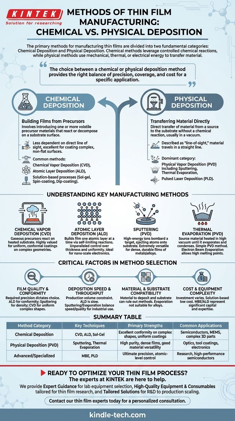
The primary methods for manufacturing thin films are divided into two fundamental categories: Chemical Deposition and Physical Deposition. Chemical methods leverage controlled chemical reactions to grow a solid film on a surface from precursor materials. Physical methods use mechanical, thermal, or electrical energy to physically transfer material from a source (a "target") onto a substrate, typically within a vacuum.
The choice between a chemical or physical deposition method is not about which is "better," but which provides the right balance of precision, coverage, and cost for a specific application. Physical methods often offer higher purity and density, while chemical methods excel at coating complex shapes uniformly.
The Two Pillars of Thin Film Deposition
All thin film manufacturing techniques fall under one of two overarching approaches. Understanding this core distinction is the first step in selecting the correct process for your needs.
Chemical Deposition: Building Films from Precursors
Chemical deposition involves introducing one or more volatile precursor materials that react or decompose on a substrate surface to produce the desired film.
This approach is less dependent on a direct line of sight between the source and the substrate, making it excellent for coating complex, non-flat surfaces.
Common methods include Chemical Vapor Deposition (CVD), Atomic Layer Deposition (ALD), and solution-based processes like sol-gel, spin-coating, and dip-coating.
Physical Deposition: Transferring Material Directly
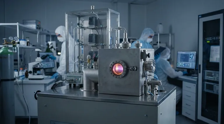
Physical deposition involves the direct transfer of material from a source to the substrate without a chemical reaction. This process is almost always performed in a vacuum chamber to ensure purity.
These methods are often described as "line-of-sight," meaning the material travels in a straight line from the source to the substrate.
The dominant category here is Physical Vapor Deposition (PVD), which includes key techniques like Sputtering, Thermal Evaporation, and Pulsed Laser Deposition (PLD).
Understanding Key Manufacturing Methods
While dozens of specific techniques exist, a few are cornerstones of modern industry, each with distinct characteristics.
Chemical Vapor Deposition (CVD)
In CVD, a substrate is exposed to gaseous precursor materials inside a reaction chamber. When these gases contact the heated substrate, they react or decompose, forming a solid, high-quality film on its surface.
It is highly valued for producing uniform, conformal coatings that can cover intricate and complex geometries with ease.
Atomic Layer Deposition (ALD)
ALD is a highly advanced form of CVD that builds a film one single atomic layer at a time. It uses a sequence of self-limiting chemical reactions, providing unparalleled control over film thickness and uniformity.
While this precision makes ALD an exceptionally slow process, it is essential for manufacturing modern high-performance semiconductors and microelectronics.
Sputtering (A PVD Method)
Sputtering involves bombarding a solid source material, known as a target, with high-energy ions inside a vacuum. This impact ejects, or "sputters," atoms from the target, which then travel and deposit onto the substrate.
This is an extremely versatile and reliable method for creating dense, durable, and highly adherent films from a vast range of materials, including metals and alloys.
Thermal Evaporation (A PVD Method)
Evaporation is one of the simplest PVD methods. The source material is heated in a high vacuum until it evaporates. These vaporized atoms then travel through the vacuum chamber and condense on the cooler substrate, forming the thin film.
Electron Beam Evaporation is a more advanced version that uses a focused electron beam to heat the material, allowing for the deposition of materials with very high melting points.
Critical Factors in Method Selection
Choosing the right deposition technique requires a careful analysis of the trade-offs between quality, speed, and cost. No single method is perfect for every scenario.
Film Quality and Conformity
The required precision dictates the choice. ALD offers the highest possible conformity and thickness control, making it ideal for nano-scale electronics. Sputtering produces very dense and pure films, while CVD is the champion for uniformly coating complex shapes.
Deposition Speed and Throughput
Production volume is a major constraint. ALD is inherently slow due to its layer-by-layer nature. Sputtering and Evaporation offer a good balance of speed and quality, making them suitable for many industrial applications from optics to tool coatings.
Material and Substrate Compatibility
The material you wish to deposit and the substrate you are coating it on can rule out certain methods. Evaporation, for example, is not suitable for alloys, as the constituent elements will evaporate at different rates.
Cost and Equipment Complexity
The financial investment varies dramatically. Solution-based methods like dip-coating can be very low-cost. In contrast, advanced systems for Molecular Beam Epitaxy (MBE) or ALD represent a significant capital expenditure and require specialized operational expertise.
Making the Right Choice for Your Application
To select the best method, you must align the process capabilities with your primary technical and business goals.
- If your primary focus is ultimate precision and uniformity: Atomic Layer Deposition (ALD) provides unparalleled control over film thickness and conformity, essential for advanced semiconductors.
- If your primary focus is coating complex 3D surfaces: Chemical Vapor Deposition (CVD) is ideal for creating uniform films that are not limited by line-of-sight.
- If your primary focus is versatility and high-density films: Sputtering is a robust workhorse for depositing a wide range of high-quality materials for optics, tools, and electronics.
- If your primary focus is speed and cost-effectiveness for simpler coatings: Thermal Evaporation or solution-based methods like spin-coating offer efficient paths for many applications.
Understanding these fundamental trade-offs empowers you to choose a manufacturing process that delivers the required performance without unnecessary complexity or cost.
Summary Table:
| Method Category | Key Techniques | Primary Strengths | Common Applications |
|---|---|---|---|
| Chemical Deposition | CVD, ALD, Sol-Gel | Excellent conformity on complex shapes, uniform coatings | Semiconductors, MEMS, complex 3D parts |
| Physical Deposition (PVD) | Sputtering, Thermal Evaporation | High purity, dense films, good material versatility | Optics, tool coatings, electronics |
| Advanced/Specialized | MBE, PLD | Ultimate precision, atomic-level control | Research, high-performance semiconductors |
Ready to Optimize Your Thin Film Process?
Choosing the right deposition method is critical for achieving the desired film quality, performance, and cost-efficiency for your specific application. The experts at KINTEK are here to help.
We provide:
- Expert Guidance: Our team will help you select the ideal lab equipment—from sputtering systems to CVD reactors—based on your material, substrate, and performance requirements.
- High-Quality Equipment & Consumables: KINTEK specializes in reliable, precision lab equipment and consumables tailored for thin film research and production.
- Tailored Solutions: Whether you're in R&D or scaling up production, we have solutions for applications in semiconductors, optics, wear-resistant coatings, and more.
Don't leave your project's success to chance. Contact our thin film experts today for a personalized consultation and discover how KINTEK can empower your laboratory's innovation.
Visual Guide
Related Products
- Aluminized Ceramic Evaporation Boat for Thin Film Deposition
- Tungsten Evaporation Boat for Thin Film Deposition
- Electron Beam Evaporation Coating Oxygen-Free Copper Crucible and Evaporation Boat
- Molybdenum Tungsten Tantalum Evaporation Boat for High Temperature Applications
- Vacuum Hot Press Furnace Machine for Lamination and Heating
People Also Ask
- Why is an alumina boat selected for catalyst precursors? Ensure Sample Purity at 1000 °C
- What are thin films deposited by evaporation? A Guide to High-Purity Coating
- What are the applications of thin films deposition? Unlock New Possibilities for Your Materials
- Why are high-purity ceramic boats used for lignin activation? Ensure Purity & Thermal Stability
- What is the widely used boat made of in thermal evaporation? Choosing the Right Material for High-Purity Deposition


