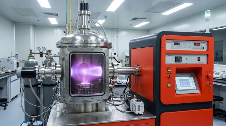
In advanced manufacturing and research, a sputtering system is a highly precise vacuum technology used to deposit ultra-thin films of material onto a surface, or substrate. The process works by creating an energized plasma that bombards a source material, known as a target, knocking atoms loose which then travel and coat the substrate. This physical, non-thermal process allows for the creation of exceptionally pure, dense, and strongly bonded layers on an atomic scale.
Sputtering is not simply a coating method; it is a foundational fabrication technique for creating high-performance materials. Its core value lies in its unparalleled control over film thickness, purity, and adhesion, making it essential for producing everything from microchips to advanced optical lenses.
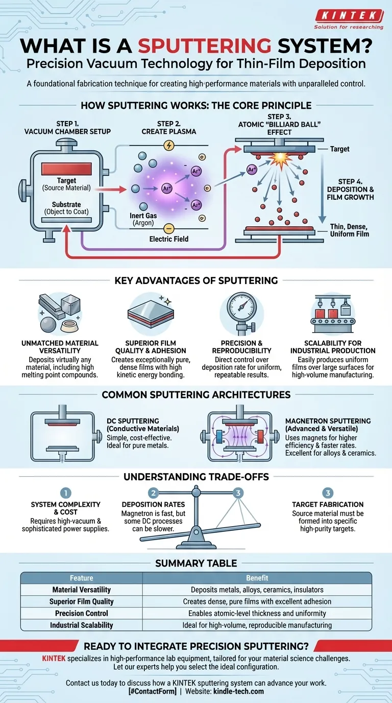
How Sputtering Works: The Core Principle
Sputtering is a physical vapor deposition (PVD) process. Unlike thermal evaporation, which boils a material, sputtering uses momentum transfer to physically eject atoms from a source.
The Target and Substrate
The process takes place inside a vacuum chamber containing two key components. The target is a solid block of the material you wish to deposit, while the substrate is the object you want to coat.
Creating the Plasma
The chamber is filled with a small amount of an inert gas, typically Argon. A strong electric field is applied, which strips electrons from the Argon atoms, creating an ionized gas or plasma composed of positive Argon ions and free electrons.
The Atomic "Billiard Ball" Effect
The positively charged Argon ions are accelerated by the electric field and slam into the negatively charged target. This high-energy collision physically knocks atoms or molecules loose from the target material, a process analogous to a cue ball breaking a rack of billiard balls.
Deposition and Film Growth
These ejected target atoms travel through the vacuum chamber and land on the substrate. As they accumulate, they form a thin, uniform, and highly dense film with exceptional adhesion, a direct result of the high kinetic energy of the arriving atoms.
Key Advantages of Sputtering Technology
Sputtering is widely adopted in high-tech industries because the films it produces have superior qualities that are difficult to achieve with other methods.
Unmatched Material Versatility
Virtually any material can be deposited via sputtering. This includes pure metals, alloys, semiconductors, and even insulators and complex compounds like ceramics that have extremely high melting points.
Superior Film Quality and Adhesion
The high energy of the sputtered atoms ensures they form a very dense, pure film with few defects or pinholes. This energy also helps them bond tenaciously to the substrate, creating a durable and long-lasting coating.
Precision and Reproducibility
The deposition rate is directly controlled by the electrical current applied to the target. This allows for extremely precise control over film thickness, ensuring that processes are highly uniform and repeatable from one run to the next.
Scalability for Industrial Production
Sputtering can easily produce uniform films over very large surface areas. This, combined with its reproducibility and fast coating rates in modern systems, makes it perfectly suited for high-volume, high-efficiency industrial manufacturing.
Common Sputtering Architectures
While the core principle remains the same, different sputtering configurations are used to optimize the process for specific materials and applications.
DC Sputtering
Direct Current (DC) sputtering is the simplest and most cost-effective form. It works exceptionally well for depositing electrically conductive materials, such as pure metals. Its straightforward nature makes it a workhorse for applications requiring basic metallic coatings on a large scale.
Magnetron Sputtering
Magnetron sputtering is a more advanced technique that uses powerful magnets behind the target. These magnets trap electrons near the target's surface, dramatically increasing the efficiency of the plasma and leading to much faster deposition rates. This method is highly versatile and can be used for a wide range of materials, including alloys and ceramics.
Understanding the Trade-offs
While powerful, sputtering is not the right solution for every problem. Understanding its limitations is key to using it effectively.
System Complexity and Cost
Sputtering systems require a high-vacuum environment and sophisticated power supplies. This makes them inherently more complex and expensive to purchase and maintain compared to simpler coating methods like electroplating or thermal evaporation.
Deposition Rates
While magnetron sputtering is quite fast, some DC sputtering processes can be slower than other deposition techniques. For applications where speed is the only concern and film quality is secondary, other methods might be more efficient.
Target Fabrication
The source material must be formed into a high-purity target of a specific size and shape to fit the system. For exotic or custom alloy materials, fabricating a suitable target can add cost and lead time to a project.
How to Apply This to Your Project
Choosing the right deposition technology depends entirely on the required properties of the final film.
- If your primary focus is cost-effective coating of pure metals: A DC sputtering system provides a simple, reliable, and high-quality solution.
- If your primary focus is high performance, alloys, or insulating compounds: Magnetron sputtering offers the necessary speed, material flexibility, and process control.
- If your primary focus is industrial-scale production with high uniformity: Sputtering's excellent reproducibility and ability to coat large areas make it a superior choice.
Ultimately, a sputtering system offers unparalleled control over the atomic-level construction of surfaces, enabling the creation of advanced materials from the ground up.
Summary Table:
| Feature | Benefit |
|---|---|
| Material Versatility | Deposits metals, alloys, ceramics, and insulators |
| Superior Film Quality | Creates dense, pure films with excellent adhesion |
| Precision Control | Enables atomic-level thickness and uniformity |
| Industrial Scalability | Ideal for high-volume, reproducible manufacturing |
Ready to integrate precision sputtering into your research or production?
KINTEK specializes in high-performance lab equipment, including sputtering systems tailored for your specific material science and fabrication challenges. Our experts can help you select the ideal configuration—from cost-effective DC sputtering for metals to advanced magnetron sputtering for complex compounds—ensuring you achieve the film quality, adhesion, and scalability your projects demand.
Contact us today to discuss how a KINTEK sputtering system can advance your work. #ContactForm
Visual Guide
Related Products
- Spark Plasma Sintering Furnace SPS Furnace
- Vacuum Induction Melting Spinning System Arc Melting Furnace
- Chemical Vapor Deposition CVD Equipment System Chamber Slide PECVD Tube Furnace with Liquid Gasifier PECVD Machine
- Customer Made Versatile CVD Tube Furnace Chemical Vapor Deposition Chamber System Equipment
People Also Ask
- What is the process fundamentals of spark plasma sintering? Achieve Rapid, High-Density Material Consolidation
- What are the fundamentals of spark plasma sintering process? Unlock Rapid, High-Performance Material Consolidation
- What is the difference between spark plasma sintering and flash sintering? A Guide to Advanced Sintering Methods
- What are the advantages of CAMI/SPS for W-Cu composite preparation? Reduce cycles from hours to seconds.
- What is the mechanism of SPS process? A Deep Dive into Rapid, Low-Temperature Sintering


