At its core, DC (Direct Current) sputtering is a widely used industrial process for creating extremely thin, high-quality films of material on a surface. It is a type of Physical Vapor Deposition (PVD) used to coat objects with a layer ranging from just a few nanometers to several micrometers thick, finding applications in everything from semiconductors and disk drives to medical tools and aerospace components.
DC sputtering is the go-to method for depositing thin films of electrically conductive materials. It is valued in industrial settings because it offers a highly effective balance of low cost, operational simplicity, and the ability to produce high-purity, uniform coatings at scale.

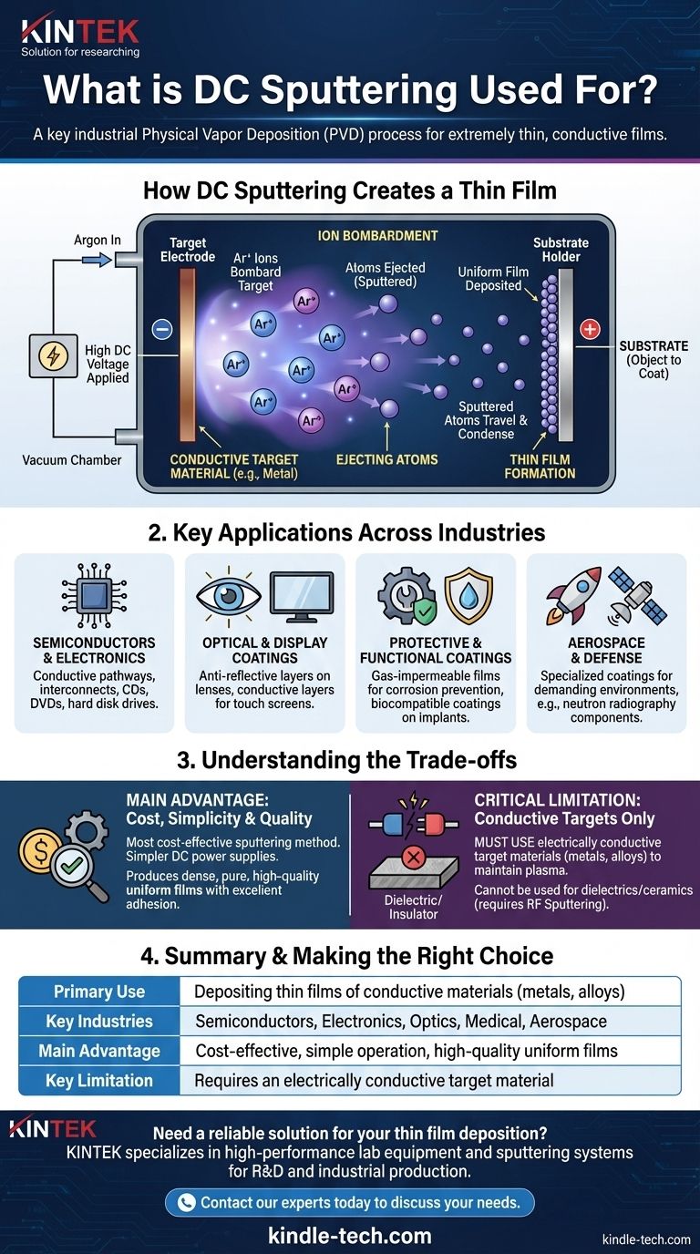
How DC Sputtering Creates a Thin Film
DC sputtering is a vacuum deposition technique. The entire process happens inside a sealed chamber from which air has been removed.
The Basic Principle: Ion Bombardment
A high DC voltage is applied between two electrodes: the target (which is made of the material you want to deposit) and the substrate (the object you want to coat).
A small amount of an inert gas, typically Argon, is introduced into the chamber. The high voltage ionizes this gas, creating a glowing plasma of positively charged Argon ions and free electrons.
Ejecting Atoms from the Target
The positively charged Argon ions are accelerated by the electric field and collide with the negatively charged target surface with great force.
This high-energy bombardment has enough force to physically knock out, or "sputter," individual atoms from the target material.
Forming a Film on the Substrate
These sputtered atoms travel through the vacuum chamber and land on the substrate, which is strategically placed to intercept them.
As these atoms accumulate, they condense and form a very thin, uniform, and dense film on the substrate's surface.
Key Applications Across Industries
The combination of low cost and high quality makes DC sputtering essential for a wide range of modern technologies.
Semiconductors and Electronics
This is one of the largest applications. DC sputtering is used to deposit the thin metallic layers that form the conductive pathways and interconnects inside integrated circuits. It's also used in manufacturing CDs, DVDs, and hard disk drives.
Optical and Display Coatings
Sputtering is used to apply thin films to glass for various optical purposes, such as creating anti-reflective layers on lenses or conductive layers for touch screens and flat-panel displays.
Protective and Functional Coatings
DC sputtering can create films that protect a surface from its environment. This includes depositing gas-impermeable films to prevent corrosion on sensitive materials or creating biocompatible coatings on medical implants.
Aerospace and Defense
The process is used to apply specialized coatings for demanding environments. For example, gadolinium films are sputtered onto components used in neutron radiography to improve imaging quality.
Understanding the Trade-offs
No single technique is perfect for every situation. Choosing DC sputtering involves understanding its primary benefits and its crucial limitation.
The Main Advantage: Cost and Simplicity
DC sputtering is the most basic and inexpensive form of sputtering. The required DC power supplies are cheaper and simpler to operate than more complex alternatives, making it highly attractive for industrial-scale production.
The Critical Limitation: Conductive Targets Only
DC sputtering can only be used with electrically conductive target materials, primarily metals. The target must be able to conduct electricity to maintain the plasma and prevent a buildup of positive charge on its surface, which would repel the Argon ions and stop the process.
This is the most important factor when choosing a sputtering method. For non-conductive (dielectric or insulating) materials like ceramics, a different technique like RF (Radio Frequency) sputtering is required.
Film Quality and Adhesion
Despite its simplicity, DC sputtering produces very high-quality films. The resulting layers are dense, pure, and exhibit excellent adhesion to the substrate, making them durable and reliable for demanding applications.
Making the Right Choice for Your Deposition Needs
To select the correct technology, you must first define your material and your primary goal.
- If your primary focus is cost-effective deposition of a metal or conductive alloy: DC sputtering is almost always the most efficient and economical choice for high-volume manufacturing.
- If your primary focus is depositing a non-conductive material (like an oxide or ceramic): You must use a different method, such as RF sputtering, as the physics of the DC process will not work.
- If your primary focus is achieving a high-purity, uniform film with excellent adhesion: DC sputtering is a highly reliable technique that delivers precise control and consistent results for conductive targets.
Ultimately, understanding the fundamental requirement for an electrically conductive target is the key to leveraging the power and efficiency of DC sputtering.
Summary Table:
| Aspect | Key Detail |
|---|---|
| Primary Use | Depositing thin films of conductive materials (metals, alloys) |
| Key Industries | Semiconductors, Electronics, Optics, Medical, Aerospace |
| Main Advantage | Cost-effective, simple operation, high-quality uniform films |
| Key Limitation | Requires an electrically conductive target material |
Need a reliable solution for your thin film deposition?
KINTEK specializes in high-performance lab equipment, including sputtering systems tailored for R&D and industrial production. Whether you are developing next-generation semiconductors or require durable protective coatings, our expertise ensures you get the precise, cost-effective results you need.
Contact our experts today to discuss how our sputtering solutions can enhance your process and product quality.
Visual Guide
Related Products
- Spark Plasma Sintering Furnace SPS Furnace
- Vacuum Induction Melting Spinning System Arc Melting Furnace
- Circulating Water Vacuum Pump for Laboratory and Industrial Use
People Also Ask
- Why are Spark Plasma Sintering (SPS) furnaces or hot presses utilized in the preparation of Li3PS4 solid electrolytes?
- What is the process fundamentals of spark plasma sintering? Achieve Rapid, High-Density Material Consolidation
- What are the advantages of CAMI/SPS for W-Cu composite preparation? Reduce cycles from hours to seconds.
- What are the fundamentals of spark plasma sintering process? Unlock Rapid, High-Performance Material Consolidation
- What technical advantages does a Spark Plasma Sintering (SPS) furnace offer for LZP ceramics? Enhance Ionic Conductivity


