At its core, sputtering is a physical vapor deposition (PVD) method used to create ultra-thin, highly uniform coatings on a surface. It is a vacuum-based process where a solid source material, called the target, is bombarded with energetic ions from a plasma. This bombardment physically knocks atoms off the target, which then travel through the vacuum and deposit onto a substrate, forming the desired film.
Sputtering is best understood as a microscopic sandblasting process. Instead of sand, it uses ionized gas in a vacuum to precisely "chip away" atoms from a source material and deposit them as an ultra-thin, highly uniform coating onto another surface.
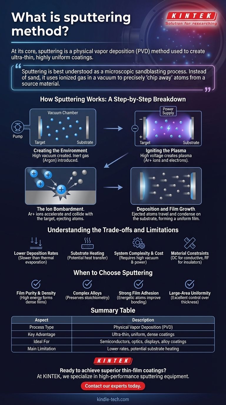
How Sputtering Works: A Step-by-Step Breakdown
To understand why sputtering is so widely used in industries from semiconductors to optics, it is crucial to understand its core mechanics. The process is a sequence of precise physical events, not a chemical reaction.
Step 1: Creating the Environment
The process begins by placing the target (the material to be deposited) and the substrate (the object to be coated) into a vacuum chamber. Air is pumped out to create a high vacuum, which prevents contamination and ensures the sputtered atoms can travel freely.
An inert gas, most commonly Argon (Ar), is then introduced into the chamber at a very low pressure.
Step 2: Igniting the Plasma
A high voltage is applied between the target and the chamber walls, with the target acting as the negative electrode (cathode). This strong electric field energizes the Argon gas, stripping electrons from the Argon atoms.
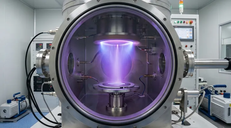
This process creates a plasma, an energized state of matter consisting of positive Argon ions (Ar+) and free electrons. This plasma often emits a characteristic glow, typically purple or blue.
Step 3: The Ion Bombardment
The positively charged Argon ions are powerfully accelerated by the electric field and drawn toward the negatively charged target. They collide with the target surface with significant kinetic energy.
Think of this as an atomic-scale game of pool. The Argon ion is the cue ball, striking the racked atoms of the target material.
Step 4: Deposition and Film Growth
When the collision cascade has enough energy to overcome the target's surface binding energy, it physically ejects atoms from the target. These ejected atoms travel through the vacuum chamber.
These sputtered atoms land on the substrate, where they condense and build up, layer by layer, to form a thin film. Because this happens at an atomic level, the process allows for exceptional control over the film's thickness, density, and uniformity.
Understanding the Trade-offs and Limitations
While powerful, sputtering is not a universal solution. An objective assessment requires understanding its inherent limitations.
Lower Deposition Rates
Compared to other methods like thermal evaporation, sputtering can be a slower process. The rate of material deposition is often lower, which can impact throughput in high-volume manufacturing.
Substrate Heating
The constant bombardment of energetic particles (including ions and sputtered atoms) transfers energy to the substrate, causing it to heat up. This can be a significant problem for coating heat-sensitive materials like plastics or certain biological samples.
System Complexity and Cost
Sputtering systems require high-vacuum chambers, sophisticated power supplies, and often magnetic confinement systems (magnetron sputtering). This makes the equipment more complex and expensive than some alternative coating methods.
Material Constraints
For the simplest form of the technique (DC sputtering), the target material must be electrically conductive. While radio frequency (RF) sputtering can be used for insulating materials, this adds another layer of complexity and cost to the system.
When to Choose Sputtering
Choosing a deposition method depends entirely on your technical and material requirements. Sputtering is the superior choice for specific goals.
- If your primary focus is film purity and density: Sputtering is an excellent choice because the high energy of deposited atoms forms dense, tightly packed films with low impurity levels.
- If your primary focus is coating complex alloys or compounds: Sputtering excels because it generally preserves the stoichiometry (the elemental ratio) of the target material in the resulting film.
- If your primary focus is achieving strong film adhesion: The energetic nature of sputtered atoms often results in better adhesion to the substrate compared to lower-energy deposition techniques.
- If your primary focus is large-area uniformity: Sputtering provides exceptional control over film thickness and uniformity, making it ideal for coating large substrates like architectural glass or displays.
By understanding its principles, you can effectively leverage sputtering to engineer materials with precisely tailored properties at the atomic level.
Summary Table:
| Aspect | Description |
|---|---|
| Process Type | Physical Vapor Deposition (PVD) |
| Key Advantage | Ultra-thin, highly uniform, and dense coatings |
| Ideal For | Semiconductors, optics, displays, alloy coatings |
| Main Limitation | Lower deposition rates and potential substrate heating |
Ready to achieve superior thin-film coatings for your laboratory?
At KINTEK, we specialize in providing high-performance sputtering equipment and consumables tailored to your specific research and production needs. Whether you are working in semiconductor fabrication, materials science, or optical coating, our solutions deliver the purity, uniformity, and adhesion your projects demand.
Contact our experts today to discuss how our sputtering systems can enhance your lab's capabilities and drive your innovations forward.
Visual Guide
Related Products
- Spark Plasma Sintering Furnace SPS Furnace
- Vacuum Induction Melting Spinning System Arc Melting Furnace
- Chemical Vapor Deposition CVD Equipment System Chamber Slide PECVD Tube Furnace with Liquid Gasifier PECVD Machine
- Customer Made Versatile CVD Tube Furnace Chemical Vapor Deposition Chamber System Equipment
People Also Ask
- What is SPS sintering method? A Guide to High-Speed, High-Performance Material Fabrication
- What is the mechanism of SPS process? A Deep Dive into Rapid, Low-Temperature Sintering
- What are the fundamentals of spark plasma sintering process? Unlock Rapid, High-Performance Material Consolidation
- What is the pressure for spark plasma sintering? A Guide to Optimizing SPS Parameters
- What is the theory of spark plasma sintering? A Guide to Rapid, Low-Temperature Densification


