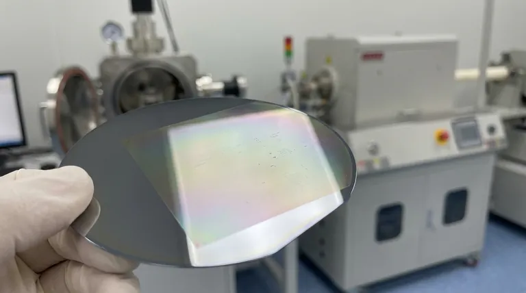
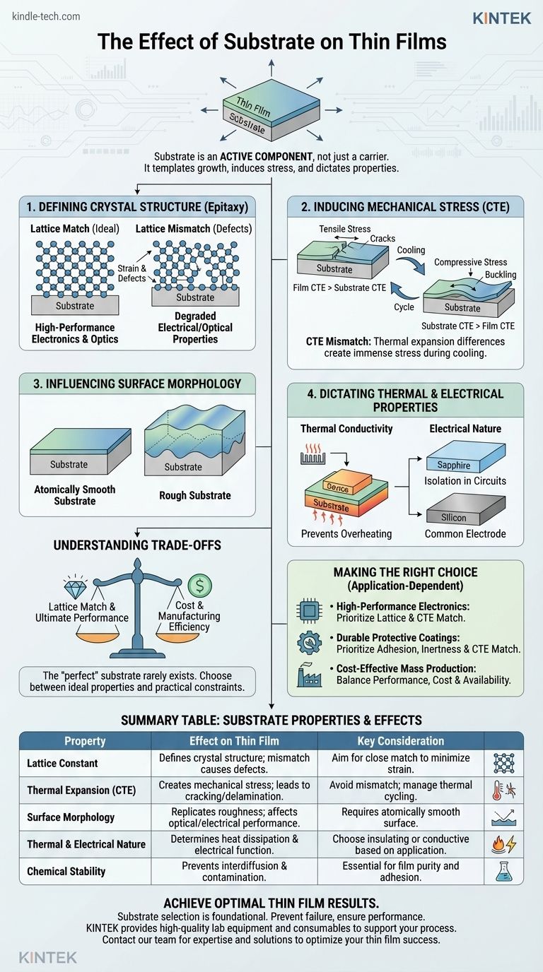
In thin film technology, the substrate is not a passive carrier but an active and critical component that fundamentally dictates the final film's structure, properties, and performance. Its influence extends from the atomic level, defining the crystalline quality of the film, to the macroscopic level, where it can introduce mechanical stress that leads to device failure. The choice of substrate is a foundational engineering decision that can determine the success or failure of the entire fabrication process.
The most critical takeaway is this: a thin film does not exist in isolation. The substrate actively templates the film's growth, induces stress, and contributes to its overall thermal and electrical behavior, making substrate selection as important as the film material itself.
The Substrate's Role: More Than Just a Foundation
Thinking of the substrate as mere physical support is a common oversimplification. In reality, it is an active participant in the film's creation, with its properties directly influencing the final product's quality and functionality.
Defining the Film's Crystal Structure
The arrangement of atoms in the substrate serves as a blueprint for the film growing on top of it, a phenomenon known as epitaxy.
When the atomic spacing of the substrate (lattice constant) closely matches that of the film material, the film can grow with a highly ordered, single-crystal structure. This is the ideal scenario for high-performance electronic and optical devices.
If there is a significant lattice mismatch, the film is forced to stretch or compress to conform to the substrate. This stored energy, or strain, is eventually relieved by creating defects like dislocations, which severely degrade the film's electrical and optical properties.
Inducing Mechanical Stress
Most thin film deposition processes occur at elevated temperatures. As the system cools, the film and substrate contract at different rates according to their unique coefficients of thermal expansion (CTE).
A mismatch in CTE creates immense mechanical stress. If the film contracts more than the substrate, it experiences tensile stress, which can lead to cracking. If the substrate contracts more, the film is put under compressive stress, which can cause it to buckle or delaminate.
Influencing Surface Morphology
The initial surface of the substrate sets the stage for the film's final texture. Any pre-existing roughness, waviness, or contamination on the substrate will be replicated or even amplified in the growing film.
For applications like mirrors or semiconductor wafers, an atomically smooth substrate is non-negotiable. A rough substrate leads to a rough film, causing issues like light scattering in optical coatings or short-circuiting in electronic devices.
Dictating Thermal and Electrical Properties
The substrate is an integral part of the final device's operational environment. Its thermal conductivity determines how effectively heat generated during operation can be dissipated. A poorly chosen substrate can lead to overheating and premature device failure.
Furthermore, the substrate's electrical nature is fundamental. An insulating substrate (like sapphire or quartz) is used to isolate different components in a circuit, while a conductive substrate (like a silicon wafer) can serve as a common electrode.
Understanding the Trade-offs in Substrate Selection
The "perfect" substrate rarely exists. The selection process is a careful balancing act between ideal physical properties and real-world manufacturing constraints like cost and availability.
The Lattice Match vs. Cost Dilemma
A substrate with a near-perfect lattice match for a specific film may be exceptionally effective but also prohibitively expensive or difficult to manufacture. For example, growing gallium nitride (GaN) on a pure GaN substrate is ideal but costly.
Consequently, engineers often compromise by using a less-ideal but far cheaper substrate, such as silicon or sapphire, and then developing complex buffer layers to manage the resulting strain and defects. This is a core trade-off between ultimate performance and manufacturing efficiency.
Thermal Compatibility vs. Functionality
You may find a substrate with an excellent CTE match, minimizing thermal stress. However, that same substrate might have the wrong electrical properties (e.g., being conductive when you need an insulator) or be chemically reactive with your film material at high temperatures.
Chemical Reactivity and Interdiffusion
At the high temperatures used in many deposition techniques, atoms are highly mobile. It is possible for atoms from the substrate to diffuse into the thin film, or vice-versa, creating an unintended interfacial layer.
This interdiffusion can contaminate the film, alter its properties, and create a weak boundary that is prone to adhesion failure. Substrate choice must therefore account for chemical stability at the intended processing temperatures.
Making the Right Choice for Your Application
Selecting the correct substrate requires you to first define your primary goal. The optimal choice is always context-dependent.
- If your primary focus is high-performance electronics or optics: Prioritize a substrate with the closest possible lattice match and thermal expansion coefficient to grow a low-defect, single-crystal film.
- If your primary focus is durable protective coatings: Prioritize strong adhesion, chemical inertness, and a CTE match that prevents cracking or delamination under thermal cycling.
- If your primary focus is cost-effective mass production: Identify a substrate that offers an acceptable balance of performance, cost, and availability, and be prepared to engineer solutions to mitigate its physical shortcomings.
Treating the substrate as an integral component of your design, not just a carrier, is the key to predictable and successful thin film engineering.
Summary Table:
| Substrate Property | Effect on Thin Film | Key Consideration |
|---|---|---|
| Lattice Constant | Defines crystal structure via epitaxy; mismatch causes defects. | Aim for close match to minimize strain and dislocations. |
| Thermal Expansion (CTE) | Creates mechanical stress (tensile/compressive) during cooling. | Mismatch can lead to cracking, buckling, or delamination. |
| Surface Morphology | Replicates roughness, affecting optical and electrical performance. | Requires atomically smooth surface for high-quality films. |
| Thermal & Electrical Nature | Determines heat dissipation and electrical isolation/connection. | Choose insulating (e.g., sapphire) or conductive (e.g., silicon) based on application. |
| Chemical Stability | Prevents interdiffusion and contamination at high temperatures. | Essential for maintaining film purity and strong adhesion. |
Achieve Optimal Thin Film Results with the Right Substrate
Substrate selection is a foundational decision that directly impacts the quality, performance, and reliability of your thin film devices. The right choice prevents issues like stress-induced failure, poor crystallinity, and contamination.
KINTEK specializes in providing high-quality laboratory equipment and consumables to support your entire thin film fabrication process. Whether you are developing high-performance electronics, durable coatings, or cost-effective mass-produced components, we offer solutions to meet your specific substrate and processing needs.
Let our expertise guide you to success. Contact our team today to discuss your application requirements and discover how we can help you select the ideal substrate and optimize your thin film processes for superior results.
Visual Guide
Related Products
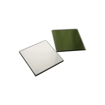
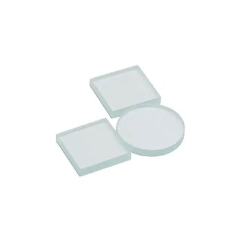
- MgF2 Magnesium Fluoride Crystal Substrate Window for Optical Applications
- Optical Window Glass Substrate Wafer Single Double Sided Coated K9 Quartz Sheet
- Optical Window Glass Substrate Wafer Quartz Plate JGS1 JGS2 JGS3
- Conductive Carbon Cloth Carbon Paper Carbon Felt for Electrodes and Batteries
- Float Soda-Lime Optical Glass for Laboratory Use
People Also Ask
- What are optical coatings made of? Metals, Dielectrics & Polymers for Light Control
- What is the process of optical coating? A Guide to High-Precision PVD Deposition
- How do high-precision temperature controllers and thermocouples influence the conversion efficiency of Magnéli phase?
- What are the substrates used in CVD? Key Materials for Thin Film Deposition
- What is the impact of substrate temperature on film properties? Optimize Density, Crystallinity & Stress