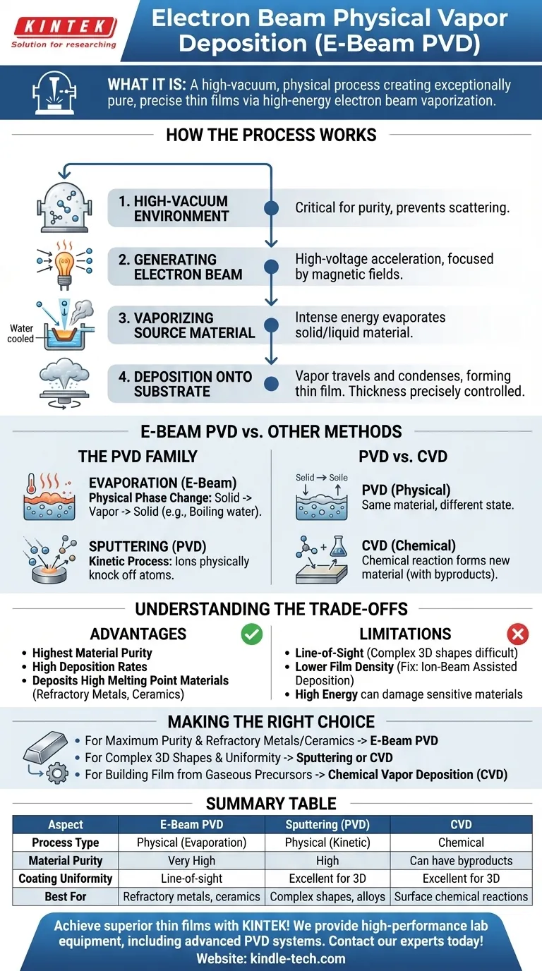
At its core, Electron Beam Physical Vapor Deposition (E-beam PVD) is a high-vacuum process used to create exceptionally pure and precise thin films. It functions by firing a high-energy beam of electrons at a source material, causing it to vaporize directly from a solid or liquid state. This vapor then travels and condenses onto a target substrate, forming a uniform coating with tightly controlled thickness.
E-beam PVD is best understood not as a chemical reaction but as a physical phase change, much like boiling water into steam that then frosts a cold window. This direct solid-to-vapor-to-solid transition allows for the deposition of very pure films from materials with extremely high melting points, which are difficult to handle with other methods.
How the E-Beam PVD Process Works
To grasp the capability of E-beam PVD, it is essential to understand the distinct steps that occur within the deposition chamber. Each stage is precisely controlled to achieve the desired film characteristics.
The High-Vacuum Environment
The entire process takes place in a chamber evacuated to a very high vacuum. This is critical to prevent the vaporized material from reacting with or being scattered by residual air molecules, ensuring the purity of the final film.
Generating the Electron Beam
A filament, typically made of tungsten, is heated to a point where it emits a stream of electrons. These electrons are then accelerated by high voltage and focused into a tight beam using magnetic fields.
Vaporizing the Source Material
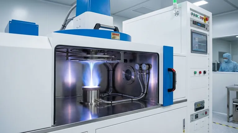
This focused, high-energy electron beam is directed onto the source material (known as the "target") held in a water-cooled crucible. The intense energy from the beam bombards the material, heating a small spot so rapidly that it evaporates or sublimates into a vapor.
Deposition onto the Substrate
The resulting vapor travels in a straight, line-of-sight path from the source to the cooler substrate, which is strategically placed above it. Upon contact with the substrate, the vapor condenses back into a solid state, forming the thin film. Computer systems precisely control the beam's power and the substrate's rotation to ensure the film grows to the pre-specified thickness and uniformity.
E-Beam PVD vs. Other Deposition Methods
E-beam PVD is one of several techniques for creating thin films. Understanding how it differs from other common methods clarifies its specific applications and advantages.
The PVD Family: Evaporation vs. Sputtering
Physical Vapor Deposition (PVD) is a category of processes that physically transfer material onto a substrate. E-beam is a form of evaporation, which uses thermal energy to "boil" material into a vapor.
The other major PVD method is sputtering, which is a kinetic process. In sputtering, a target is bombarded with high-energy ions that physically knock atoms off its surface, which then deposit onto the substrate.
The Fundamental Difference: PVD vs. CVD
The most significant distinction is between PVD and Chemical Vapor Deposition (CVD). PVD is a physical process. The deposited material is the same as the source material, just in a different state.
CVD, by contrast, is a chemical process. It introduces gaseous precursor chemicals into a chamber that then react on the substrate's surface to form an entirely new solid material, leaving behind chemical byproducts.
Understanding the Trade-offs of E-Beam PVD
Like any specialized technology, E-beam PVD has a distinct set of strengths and weaknesses that make it ideal for certain applications and less suitable for others.
Key Advantages
E-beam PVD offers some of the highest material purity available because it does not require carrier gases and involves a direct physical transition.
It can achieve very high deposition rates, making it efficient for production. Its primary advantage is the ability to deposit materials with exceptionally high melting points, such as refractory metals and ceramics, that cannot be evaporated by simple heating.
Potential Limitations
The process is line-of-sight, meaning the vapor travels in a straight line. This can make it difficult to uniformly coat complex, three-dimensional shapes without sophisticated substrate rotation and tilting mechanisms.
The resulting film density can sometimes be lower than films created by sputtering. However, this can be overcome with a technique called ion-beam assisted deposition (IBAD), where an ion beam bombards the growing film to make it denser and more robust.
Finally, the high energy involved can sometimes decompose certain compound materials or damage particularly sensitive substrates.
Making the Right Choice for Your Goal
Selecting a deposition technique depends entirely on the material you are using and the film properties you need to achieve.
- If your primary focus is maximum material purity and depositing refractory metals or ceramics: E-beam PVD is often the superior choice due to its direct, high-energy vaporization method.
- If your primary focus is coating complex 3D shapes with excellent uniformity: Sputtering or a CVD process might offer better coverage and is worth investigating.
- If your primary focus is to build a film from gaseous precursors via a surface chemical reaction: Chemical Vapor Deposition (CVD) is the correct process category to explore.
Understanding these fundamental differences empowers you to select the precise tool for your material engineering challenge.
Summary Table:
| Aspect | E-Beam PVD | Sputtering (PVD) | CVD |
|---|---|---|---|
| Process Type | Physical (Evaporation) | Physical (Kinetic) | Chemical |
| Material Purity | Very High | High | Can have byproducts |
| Coating Uniformity | Line-of-sight (requires rotation) | Excellent for 3D shapes | Excellent for 3D shapes |
| Best For | Refractory metals, ceramics | Complex shapes, alloys | Surface chemical reactions |
Ready to achieve superior thin films with E-beam PVD technology?
At KINTEK, we specialize in providing high-performance lab equipment, including advanced PVD systems, to meet the precise demands of your research and production. Whether you are working with refractory metals, ceramics, or other high-purity materials, our expertise can help you optimize your deposition process for exceptional results.
Contact our experts today to discuss your specific application and discover how KINTEK's solutions can enhance your laboratory's capabilities.
Visual Guide
Related Products
- Electron Beam Evaporation Coating Oxygen-Free Copper Crucible and Evaporation Boat
- RF PECVD System Radio Frequency Plasma-Enhanced Chemical Vapor Deposition RF PECVD
- Chemical Vapor Deposition CVD Equipment System Chamber Slide PECVD Tube Furnace with Liquid Gasifier PECVD Machine
- Electron Beam Evaporation Coating Gold Plating Tungsten Molybdenum Crucible for Evaporation
- HFCVD Machine System Equipment for Drawing Die Nano-Diamond Coating
People Also Ask
- What is the voltage of e-beam evaporation? Achieve Precise Thin-Film Deposition
- What is e-beam evaporation? Achieve High-Purity Thin Film Deposition for Your Lab
- What are the applications of e-beam evaporation? Achieve High-Purity Coatings for Optics & Electronics
- What is the current of e-beam evaporation? A Guide to High-Purity Thin Film Deposition
- What is the container that holds the metal source material called in e-beam evaporation? Ensure Purity and Quality in Your Thin-Film Deposition


