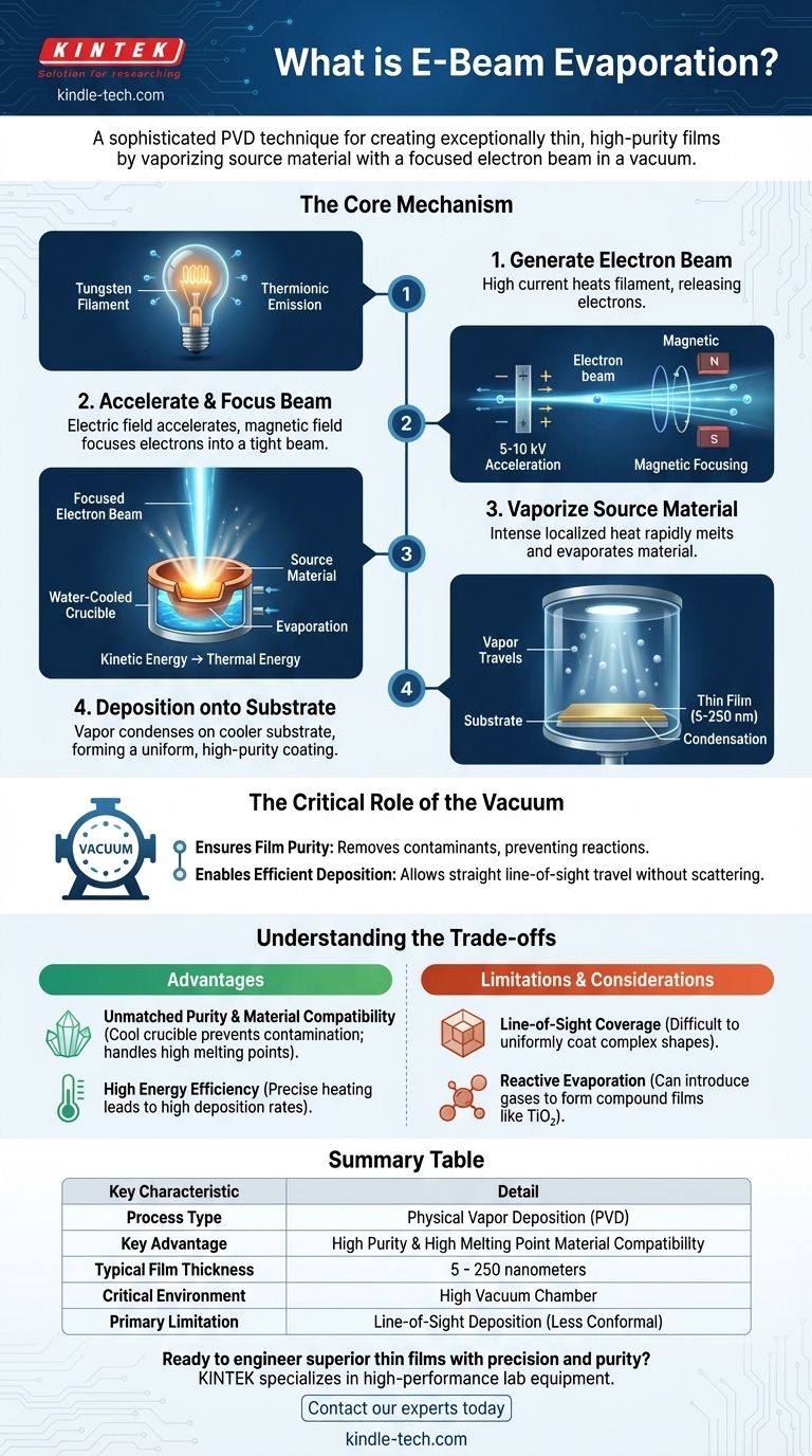
At its core, electron beam evaporation is a sophisticated technique for creating exceptionally thin, high-purity films. It is a type of Physical Vapor Deposition (PVD) where a source material, held in a vacuum, is heated by a focused, high-energy electron beam until it vaporizes. This vapor then travels and condenses onto a substrate, forming a uniform coating.
While many methods exist to create thin films, electron beam evaporation is distinguished by its precision and purity. It uses a "clean" energy source—electrons—to directly heat only the target material, avoiding the contamination common with other thermal techniques.
The Core Mechanism: From Electron to Film
To understand the value of e-beam evaporation, we must first break down the process into its fundamental steps. Each stage is precisely controlled to ensure the final film meets demanding specifications.
Step 1: Generating the Electron Beam
The process begins with a tungsten filament. A high electric current is passed through this filament, heating it to an extreme temperature. This intense heat causes thermionic emission, the release of electrons from the filament's surface.
Step 2: Accelerating and Focusing the Beam
Once freed, these electrons are accelerated by a powerful electric field, typically between 5 to 10 kilovolts (kV). A magnetic field is then used to focus these high-velocity electrons into a tight, precise beam, guiding them toward the target.
Step 3: Vaporizing the Source Material
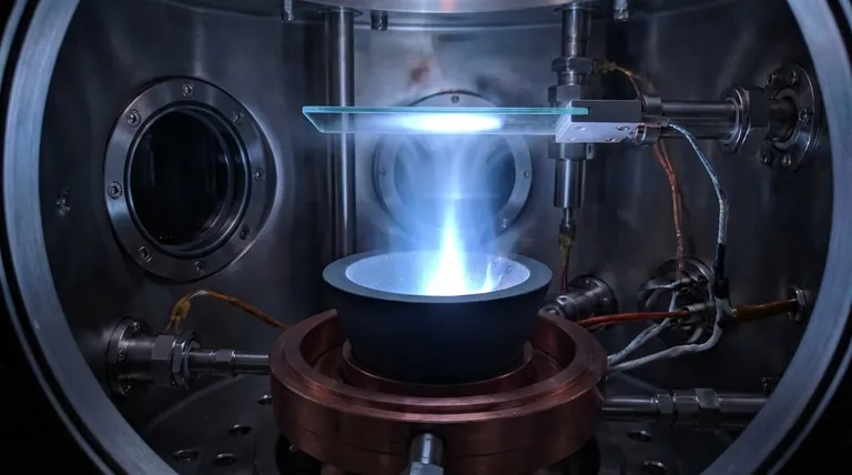
The source material to be deposited is held in a water-cooled copper hearth or crucible. When the focused electron beam strikes the material, the immense kinetic energy of the electrons is instantly converted into thermal energy. This localized heating is so intense that it causes the material to rapidly melt and evaporate (or sublimate, turning directly from a solid to a gas).
Step 4: Deposition onto the Substrate
This gaseous vapor travels upward through the vacuum chamber. It eventually reaches the cooler substrate, which is strategically positioned above the source. Upon contact, the vapor condenses back into a solid, forming a thin, dense, and highly pure film on the substrate's surface, typically between 5 and 250 nanometers thick.
The Critical Role of the Vacuum
The entire e-beam evaporation process occurs within a high-vacuum chamber. This controlled environment is not incidental; it is essential for two key reasons.
Ensuring Film Purity
The vacuum removes virtually all other gas molecules, such as oxygen and nitrogen, from the chamber. This prevents the evaporated material from reacting with contaminants during its journey, which is critical for achieving a high-purity film.
Enabling Efficient Deposition
In a vacuum, vapor particles can travel from the source to the substrate in a straight, uninterrupted path. This is known as line-of-sight deposition. Without a vacuum, the particles would collide with air molecules and scatter, preventing the formation of a uniform film.
Understanding the Trade-offs
Like any specialized process, e-beam evaporation has distinct advantages and limitations that make it suitable for specific applications.
Advantage: Unmatched Purity and Material Compatibility
Because the electron beam heats the source material directly, the surrounding crucible remains cool. This prevents the crucible material itself from melting or outgassing, which would contaminate the film. This allows the technique to be used with a vast range of materials, including those with very high melting points (refractory metals) that are difficult to evaporate by other means.
Advantage: High Energy Efficiency
The energy is delivered precisely where it's needed—on the surface of the source material. This makes the process highly efficient, enabling high deposition rates and excellent control over the film's thickness.
Limitation: Line-of-Sight Coverage
The straight-line path of the vapor particles makes it difficult to uniformly coat complex, three-dimensional shapes with sharp corners or undercuts. The parts of the substrate not in the direct line of sight of the source will receive little to no coating.
Consideration: Reactive Evaporation
This limitation can also be an opportunity. By intentionally bleeding a controlled amount of a reactive gas (like oxygen or nitrogen) into the chamber, it's possible to form compound films. For example, evaporating titanium in an oxygen atmosphere can create a titanium dioxide (TiO₂) film.
Making the Right Choice for Your Goal
Selecting a deposition method depends entirely on the desired properties of the final film and the geometry of your substrate.
- If your primary focus is maximum film purity and density: E-beam is an excellent choice because the water-cooled crucible and direct heating mechanism minimize contamination.
- If you need to deposit high-melting-point or refractory materials: The intense, localized heating of the electron beam makes it one of the most effective methods available.
- If you are creating optical coatings or advanced semiconductors: The precise thickness control and high purity offered by e-beam evaporation are essential for these applications.
- If you are coating complex 3D parts with uniform thickness: You may need to incorporate substrate rotation or consider a more conformal method like sputtering.
Ultimately, electron beam evaporation provides an unparalleled level of control and purity for engineering high-performance thin films.
Summary Table:
| Key Characteristic | Detail |
|---|---|
| Process Type | Physical Vapor Deposition (PVD) |
| Key Advantage | High Purity & High Melting Point Material Compatibility |
| Typical Film Thickness | 5 - 250 nanometers |
| Critical Environment | High Vacuum Chamber |
| Primary Limitation | Line-of-Sight Deposition (Less Conformal) |
Ready to engineer superior thin films with precision and purity? The electron beam evaporation process is ideal for demanding applications in semiconductor fabrication, optical coatings, and R&D. KINTEK specializes in providing high-performance lab equipment and consumables to meet your specific deposition needs. Contact our experts today to discuss how our solutions can enhance your laboratory's capabilities and drive your projects forward.
Visual Guide
Related Products
- Electron Beam Evaporation Coating Oxygen-Free Copper Crucible and Evaporation Boat
- Electron Beam Evaporation Coating Tungsten Crucible and Molybdenum Crucible for High Temperature Applications
- Electron Beam Evaporation Coating Gold Plating Tungsten Molybdenum Crucible for Evaporation
- E Beam Crucibles Electron Gun Beam Crucible for Evaporation
- Electron Beam Evaporation Coating Conductive Boron Nitride Crucible BN Crucible
People Also Ask
- How is an electron beam evaporator cooled during deposition? Essential Thermal Management for Stable Processes
- What is e-beam evaporation used for? Precision Coating for Optics, Aerospace & Electronics
- What is the voltage of e-beam evaporation? Achieve Precise Thin-Film Deposition
- What are the applications of electron beams? From Nanoscale Imaging to Industrial Manufacturing
- What are the applications of e-beam evaporation? Achieve High-Purity Coatings for Optics & Electronics


