At its core, Physical Vapor Deposition (PVD) is a vacuum-based process for creating high-performance thin films. It works by transitioning a source material from a solid or liquid state into a vapor, transporting that vapor across a vacuum chamber, and allowing it to condense back into a solid film on the surface of a target object, known as a substrate. This atom-by-atom transfer allows for exceptional control over the film's properties.
PVD is not a single technique but a category of processes that physically move material from a source to a substrate without a chemical reaction. Understanding the two primary methods—evaporation and sputtering—is the key to unlocking its potential for your application.
The Three-Step PVD Process
All PVD processes, regardless of the specific technique, follow the same fundamental sequence of events inside a vacuum chamber. The vacuum is critical as it prevents the vaporized material from reacting with or being scattered by atmospheric gases.
1. Generation: Creating the Vapor
The process begins by converting a solid source material, known as the "target," into a gaseous vapor. This is achieved through purely physical means, most commonly by either heating the material until it evaporates or by bombarding it with high-energy ions.
2. Transport: Traveling to the Substrate
Once vaporized, the atoms or molecules travel in a straight line through the vacuum chamber. This "line-of-sight" travel is a defining characteristic of PVD. The absence of air means there are minimal particles to collide with, ensuring the vapor reaches the substrate with high purity.
3. Deposition: Building the Film
When the vapor stream reaches the cooler substrate, it condenses back into a solid state. This forms a thin, dense, and tightly bonded film on the substrate's surface, building up layer by layer with atomic precision.
The Two Dominant PVD Methods
While the three-step process is universal, the method used to generate the vapor defines the specific PVD technique. The two most common are thermal evaporation and sputtering.
Thermal Evaporation
In this method, the source material is heated in the vacuum until it boils or sublimates directly into a vapor. A common advanced technique is e-beam evaporation, where a high-energy electron beam is used to heat the material, allowing for the deposition of materials with very high melting points, such as those used for aerospace components.
Sputtering
Sputtering uses kinetic energy instead of heat. A high-voltage electric field energizes a gas (typically argon) into a plasma. The ions from this plasma are accelerated and collide with the source material, physically knocking atoms off its surface like microscopic billiard balls. These ejected atoms then travel to and coat the substrate.
Understanding the Trade-offs: PVD vs. CVD
A common point of confusion is the difference between PVD and its counterpart, Chemical Vapor Deposition (CVD). Clarifying this distinction is crucial for making informed technical decisions.
The "Physical" in PVD
As the name implies, PVD is a physical process. The material that ends up on the substrate is the same material that left the source target; it has only changed its physical state from solid to vapor and back to solid. This makes it ideal for depositing pure metals, alloys, and certain compounds.
The "Chemical" in CVD
In contrast, Chemical Vapor Deposition (CVD) involves a chemical reaction on the substrate surface. Precursor gases are introduced into a chamber, and they react to form an entirely new solid material as the film. This process is not limited by line-of-sight and can produce highly uniform coatings on complex shapes.
Why PVD Matters: Key Applications
The precise control and high quality of PVD films make them essential in numerous high-tech industries.
Enhancing Durability and Wear Resistance
PVD is widely used to apply hard, corrosion-resistant coatings to cutting tools, dies, and machine parts. These coatings dramatically increase the lifespan and performance of tools used in harsh industrial environments.
Creating High-Performance Optical Films
The ability to control film thickness with extreme precision makes PVD ideal for optical applications. It's used to create anti-reflective coatings on lenses, conductive films for solar panels, and layers within semiconductor devices.
Ensuring Thermal and Corrosion Protection
In the aerospace industry, PVD coatings provide a dense thermal barrier on engine components. This enhances their ability to withstand extreme temperatures and improves overall durability and fuel efficiency.
Making the Right Choice for Your Goal
Selecting the correct deposition method depends entirely on the desired properties of the final film and the nature of the substrate.
- If your primary focus is coating a temperature-sensitive substrate or achieving excellent film adhesion: Sputtering is often preferred as it is a more energetic process that can be performed at lower temperatures.
- If your primary focus is achieving the highest possible film purity or a very high deposition rate: Thermal evaporation is an excellent choice, as it doesn't require a process gas like argon that could become trapped in the film.
- If your primary focus is creating a perfectly uniform (conformal) coating over a highly complex 3D shape: You should investigate Chemical Vapor Deposition (CVD), as its gas-phase reaction is not limited by line-of-sight.
By understanding these fundamental principles, you can select the precise deposition strategy to achieve your desired material properties.
Summary Table:
| PVD Aspect | Key Detail |
|---|---|
| Process Type | Physical (no chemical reaction) |
| Environment | Vacuum Chamber |
| Core Steps | 1. Vapor Generation 2. Vapor Transport 3. Film Deposition |
| Primary Methods | Thermal Evaporation & Sputtering |
| Key Characteristic | Line-of-sight deposition |
| Common Applications | Wear-resistant coatings, optical films, thermal barriers |
Ready to integrate PVD technology into your laboratory workflow? KINTEK specializes in high-quality lab equipment and consumables for all your deposition needs. Whether you are developing new materials or enhancing product durability, our expertise can help you select the right PVD solution to achieve superior film quality, adhesion, and performance. Contact our experts today to discuss how we can support your specific application goals.
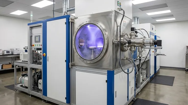
Visual Guide

Related Products
- Chemical Vapor Deposition CVD Equipment System Chamber Slide PECVD Tube Furnace with Liquid Gasifier PECVD Machine
- RF PECVD System Radio Frequency Plasma-Enhanced Chemical Vapor Deposition RF PECVD
- 915MHz MPCVD Diamond Machine Microwave Plasma Chemical Vapor Deposition System Reactor
- HFCVD Machine System Equipment for Drawing Die Nano-Diamond Coating
- Customer Made Versatile CVD Tube Furnace Chemical Vapor Deposition Chamber System Equipment
People Also Ask
- How expensive is chemical vapor deposition? Understanding the True Cost of High-Performance Coating
- What happens during deposition chemistry? Building Thin Films from Gaseous Precursors
- What is plasma enhanced chemical vapor deposition PECVD equipment? A Guide to Low-Temperature Thin Film Deposition
- What types of substrates are used in CVD to facilitate graphene films? Optimize Graphene Growth with the Right Catalyst
- How are carbon nanotubes grown? Master Scalable Production with Chemical Vapor Deposition


